摘要
Differential gain and phase (DG and DP) are common video specifications. What are they? Why are they used if they cannot be seen? This application note answers these questions, and explains how these specifications are applied to other nonvideo amplifiers, ADCs, and DACs.
A similar article was published February 18, 2011 in Planet Analog.
Technology Update
In the four years since the article was written, the video world has undergone major changes. High definition (HD) in many forms has replaced encoded systems like NTSC and PAL. The information is still relevant because of the existing installed base and of new industrial and security systems where a single coax connection is convenient.
Differential phase (DP) only applies to encoded systems with a reference burst. So with most HD, there is no DP. However, differential gain (DG) was first a black-and-white TV test. It is also a good way to explore the linearity of analog amplifiers for applications other than television. Figure 1 is a low-frequency staircase with a high frequency superimposed. Placing a small high-frequency sine wave (about 2/3 to 3/4 of the system bandwidth) on top of a larger lower-frequency sine wave will have the same effect. If the pair of signals is low level and centered between the power rails (the sweet spot), the output will have the best linearity (Figure 2). As the low-frequency signal increases in amplitude, the high-frequency signal will distort first. The second and even harmonics will increase if the distortion is asymmetrical top-to-bottom. If the signal distorts evenly top and bottom, the third and odd harmonics will increase.
Introduction
Many say that video differential gain and phase (DG and DP) are not visible to the human eye. So why would anyone want to measure something that is invisible? How are DG and DP applied to amplifiers, analog-to-digital converters (ADCs), and digital-to-analog converters (DACs)? This application note will explain how one can actually "see" (measure) DG and DP and why the specifications are important.
How Can One See DG and DP?
A DG or DP video error means that a person's flesh tone will change as he or she moves from a brightly lit area to a dimly lit area. The gain change would alter the saturation or how vivid the color is, much like the chroma control on a TV. The phase will change the hue of the color (toward green or purple) like the tint control of a NTSC (North America and Japan) TV set. So while DG and DP do indeed exist, they are said to be "invisible" because the magnitude of change is usually small. Moreover, the fluctuating scene brightness masks the errors.
Why Are DG and DP Specifications Needed?
Think of how a TV program is created. Multiple camera signals are switched and sent through special-effects equipment, then recorded, played back, and edited on the way to becoming a program. The program can be distributed over long distances by microwave, fiber optics, or satellite to eventually be broadcast over the air. A cable or satellite system then brings the program into homes so viewers can enjoy it. In this process, the video may pass through hundreds of amplifiers. Each amplifier contributes a small amount of DG and DP. To be sure that the integrity of the video signal is preserved, engineers designed a very sensitive test signal. For example, a MAX4380 amplifier is specified with a low typical DG of 0.02% and DP of 0.08 degrees.
All amplifiers have some amount of nonlinear amplitude response. Negative feedback is utilized to reduce this nonlinearity. DG and DP are really specialized linearity measurements that account for frequency response. NTSC (US) and PAL (UK, Europe, and China) TV systems send the color information on a subcarrier (3.58MHz for NTSC, 4.43MHz for PAL). DG is defined as the change in amplitude of the high-frequency subcarrier when there is change in low-frequency video level or brightness. Figure 1 shows an NTSC video waveform. The 3.58MHz subcarrier is superimposed on a lower frequency luminance signal with five brightness steps. The subcarrier is drawn as single large sine waves for clarity. In fact, there are more than 200 subcarrier cycles across one horizontal line.
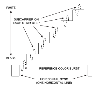
Figure 1. Video DG and DP.
DP is defined as the change in phase of the high-frequency subcarrier when the lower frequency video level or brightness changes in NTSC and PAL. The hue or tint of the color displayed is controlled by the phase relationship between the reference burst located in the black region of the video and the subcarrier present in the active video picture time. If the proper color is to be displayed, the phase must be accurately controlled.
Amplifiers, ADCs, and DACs have a "sweet spot" where they are most linear and meet the highest specifications or standards. This sweet spot is usually located midway between the two power rails (Figure 2), although the IC designer could place it at another point if necessary. Here the amplifier is operating with the best control over feedback and is naturally most linear. That means that, as a signal approaches the power-supply rails, the linearity is reduced. Superimposing a high-frequency sine wave on a low-frequency signal allows all of the amplifier's operating range to be explored. For example, if the application needs a 10MHz signal, an amplifier like the MAX4389 can be used by applying a 7MHz sine wave and then changing the DC bias. The sine-wave signal biased to midrange DC will have the best response. As the DC is changed to move the sine wave toward either power-supply rail, the sine-wave amplitude will change. Usually the high-frequency response is reduced as the power rail is approached and the transistor operating current is reduced. At the extreme condition the amplifier simply runs out of current, stops operating, and clipping occurs. ADCs and DACs can be checked in a similar manner.
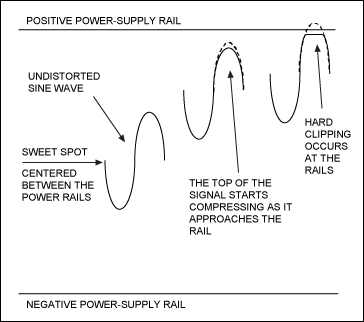
Figure 2 Amplifier DG and DP near the power rails.
As an IC becomes more complex and is more than just a single amplifier, more DG and DP error is expected. The MAX7428 video filter and buffer is specified at typical DG 0.2% and DP of 0.2 degrees. The video path is significantly more complicated as the video passes multiplex switches, a 6-pole Sallen-Key filter, and video buffer. That Sallen-Key filter is actually three or more amplifier stages.
Conclusion
So return to the original question: why measure something that cannot be seen? The DG and DP tests were designed to detect very small errors before that error could bother a human. This ensures good video quality when the video passes through hundreds of amplifiers in succession. For amplifiers, ADCs, and DACs, the performance can be verified both at the sweet spot and near the power rails. Again this process detects very small errors, thus ensuring signal integrity with multiple stages.
Maxim's complete list of op amps is available on the website.
关联至此文章
产品
1.8V、超低功耗、DirectDrive视频滤波放大器,提供负载检测
四通道、标清视频滤波器
标准清晰度、视频重建滤波器及缓冲器
SOT23封装、低噪声、低失真、宽带、满摆幅运算放大器
超低失调/漂移、低噪声、高精度、SOT23封装放大器
1MHz、20µA、满摆幅输入/输出运算放大器,带有关断
超小型、低成本、85MHz运算放大器,带有满摆幅输出及禁止功能
高输出驱动、10MHz、10V/µs、满摆幅输入/输出运算放大器,带有关断,SC70封装
单/双/四路、宽带、低功耗、单电源、满摆幅输入/输出运算放大器
200kHz、4µA、满摆幅输入/输出运算放大器,带有关断
超小型、低成本、210MHz、单电源运算放大器,带有满摆幅输出及禁止功能
SOT23封装、低噪声、低失真、宽带、满摆幅运算放大器
双路、10位、300Msps DAC,带有4倍/2倍/1倍插值滤波和PLL
双路、10位、40MHz、电流/电压输出、同时刷新DAC
非易失、四路、8位DAC,带有2线串行接口
双路、10位、可编程、可提供30mA高输出电流的DAC
32路、14位、电压输出DAC,串行接口
300Msps、12位DAC,互补电压输出
双路、超低功耗、10位、电压输出DAC
带缓冲、快速建立、八通道、12/10/8位、电压输出DAC
低成本、电压输出、16位DAC,µMAX封装
双路、8位、40Msps、3V、低功耗ADC,内置电压基准及复用并行输出
低成本、低功耗、8位DAC,带有3线串行接口,SOT23封装
8通道和4通道、±3V x VREF多量程输入、串行16位ADC
低功耗、8通道、串行12位ADC
14位、4路、软件可编程、多量程、同时采样ADC
双路、8位、100Msps、3.3V、低功耗ADC,内置电压基准及并行输出
1Msps、微处理器接口兼容、8位ADC,带有1µA关断模式
双路、10位、120Msps、3.3V、低功耗ADC,内置电压基准及并行输出
10位、105Msps、单路+3.3V、低功耗ADC,内置电压基准
双路、96Msps、14位、IF/基带ADC
10位、60Msps、3.0V、低功耗ADC,内置电压基准
150ksps、16位ADC,3.3V单电源供电
超低功耗、45Msps、双路、8位ADC
标清视频滤波放大器,提供双通道SPST开关
低成本、6通道SD以及HD/SD可选的视频滤波和缓冲器
产品分类
{{modalTitle}}
{{modalDescription}}
{{dropdownTitle}}
- {{defaultSelectedText}} {{#each projectNames}}
- {{name}} {{/each}} {{#if newProjectText}}
-
 {{newProjectText}}
{{/if}}
{{newProjectText}}
{{/if}}
{{newProjectTitle}}
{{projectNameErrorText}}
最新视频 21