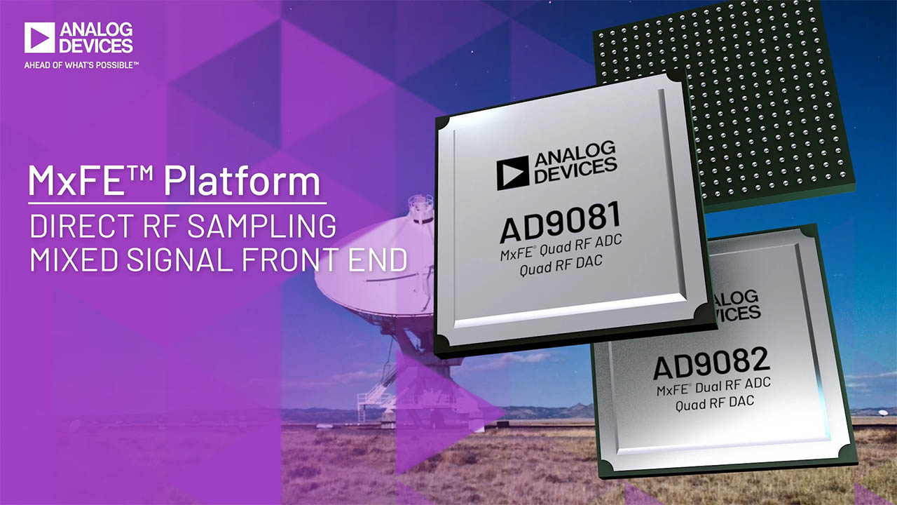
AD9084
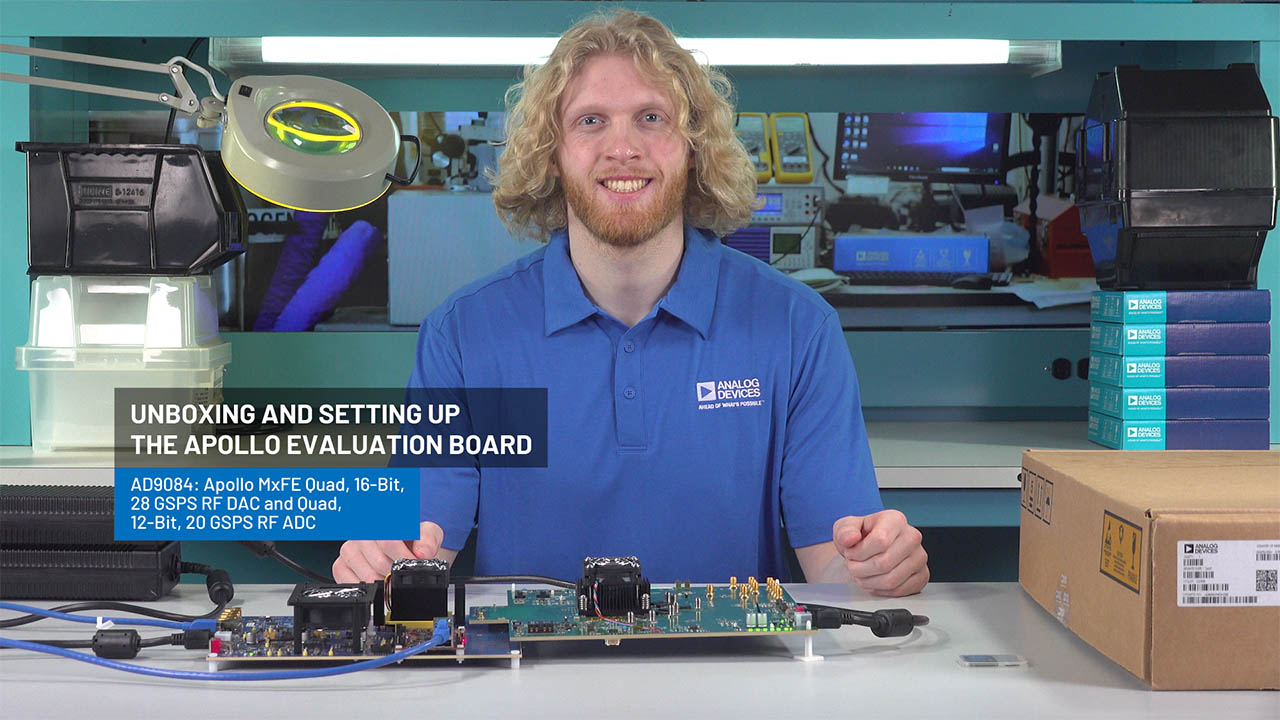
PRE-RELEASEApollo MxFE Quad, 16-Bit, 28 GSPS RF DAC and Quad, 12-Bit, 20 GSPS RF ADC
Part Details
- Flexible reconfigurable common platform design
- 4 DACs and 4 ADCs (4D4A)
- Usable RF Analog bandwidth up to 18 GHz
- Maximum DAC/ADC sample rate up to 28 GSPS/20 GSPS
- DAC to ADC sample rate ratios of 1 and 2
- Clocking
- On-chip PLL (7 GHz to 14 GHz)
- External RFCLK input up to 20 GHz
- Multichip synchronization via subclass1
- Single-ended (SE) or differential (DIFF) ADC inputs
- Two separate versions, both 50 Ω input impedance
- Single-ended version with on-chip wide bandwidth balun
- Differential ADC AC performance at 20 GSPS
- Full-scale input voltage: 500 mV p-p/−2 dBm
- Noise density: −150 dBFS/Hz at −20 dBFS at 2 GHz
- HD2/HD3: −65 dBFS/−70 dBFS at −7 dBFS at 2 GHz
- IMD3: −75 dBFS at – 13 dBFS/tone at 2 GHz
- DAC AC performance at 28 GSPS
- Full-scale output power: −2.1 dBm at 2 GHz
- IMD3: −75 dBc at – 13 dBFS/tone at 2 GHz to 10 GHz
- NSD (shuffling disabled): −164 dBFS/Hz at 0 dBFS at 2 GHz
- Versatile digital features
- Supports real or complex digital data (8-, 12-, 16-bit)
- Configurable DDC and DUC
- 8 fine complex DUCs and 4 coarse complex DUCs
- 8 fine complex DDCs and 4 coarse complex DDCs
- Option to bypass fine and coarse DUC/DDC
- DUC/DDC alias rejection
- 85 dB for interpolation filters
- 100 dB for decimation filters
- Fractional sample rate converter (FSRC)
- Programmable FIR filters for transmit/receive
- Multiple loopback (ADC to DAC) supported
- ~45 ns without DSP path
- Dynamic configuration through SPI/HSCI/GPIO
- Spectrum sniffer/monitor
- Interfaces
- SPI
- High-Speed Control Interface (HSCI)
- JESD204B/JESD204C: 20 Gbps/32.5 Gbps
- 24 lanes for Rx, 24 lanes for Tx
- Receive AGC support
- Fast detect with low latency for fast AGC control
- Signal monitor for slow AGC control
- Auxiliary features
- Power amplifier downstream protection circuitry
- On-chip temperature monitoring unit
- TDD power savings option
- Total power consumption range dependent on device configuration: 20 W to 30 W
- 24 mm × 26 mm, 899-ball BGA with 0.8 mm pitch
- Operating junction temperature (TJ): −40°C to +110°C
The Apollo mixed signal front-end (MxFE®) is a highly integrated device with a 16-bit, 28 GSPS maximum sample rate, RF digital-to-analog converter (DAC) core, and 12-bit, 20 GSPS maximum sample rate, RF analog-to-digital converter (ADC) core. The AD9084 supports four transmit channels and four receive channels. The AD9084 is well suited for applications requiring both wideband ADCs and DACs to process signal(s) having wide instantaneous bandwidth. The device features a 48 lane, 32.5 Gbps JESD204C or 20 Gbps JESD204B data transceiver port, an on-chip clock multiplier, and a digital signal processing (DSP) capability targeted at either wideband or multiband, direct to RF applications. The AD9084 also features a bypass mode that allows the full bandwidth capability of the ADC and/or DAC cores to bypass the DSP datapaths. The device also features low latency loopback and frequency hopping modes targeted at phased array radar systems and electronic warfare applications.
The AD9084 is available in a 24 mm x 26 mm, 899-ball BGA and operates within the –40°C to +110°C junction temperature range. For additional information, contact ApolloSupport@analog.com.
APPLICATIONS
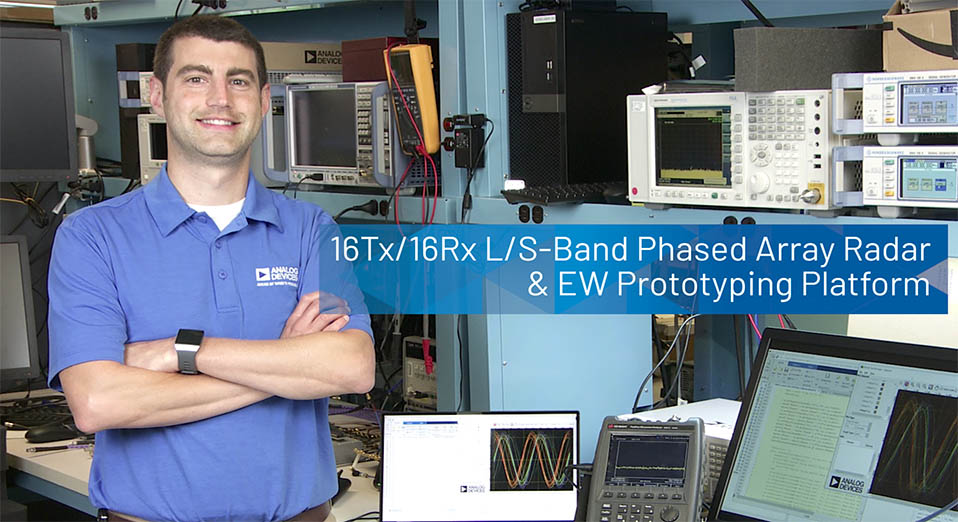
- Radar and communications
- L/S/C/X/Ku band radar and electronic warfare
- Phase array system
- Broadband communications systems
- Electronic test and measurement systems
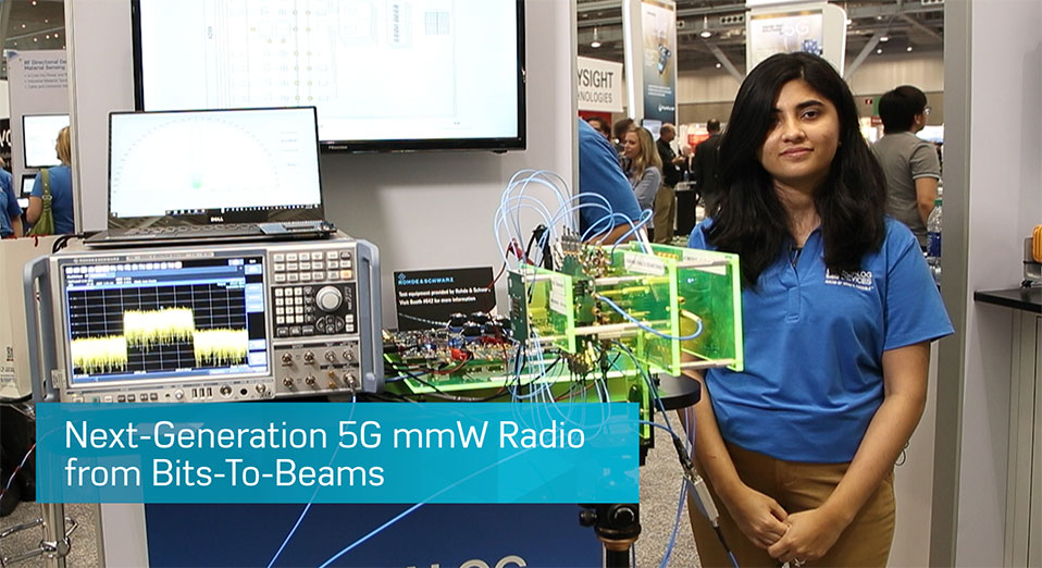
- Satellite communications
- Microwave point-to-point, X-band and 5G mmWave
Thank you for showing interest in Apollo MxFE™ and our upcoming AD9084/AD9088 product release! Subscribe to stay on top of Apollo news, TODAY!
Documentation
Data Sheet 2
User Guide 2
Application Note 1
Design Note 1
Technical Articles 19
Video 19


Product Selection Guide 1
3rd Party Solutions 1
FPGA Interoperability Reports 5
Device Drivers 4
Analog Dialogue 3
Webcast 2
Video Series 1
This is the most up-to-date revision of the Data Sheet.
Software Resources
API Device Drivers 1
Device Application Programming Interface (API) C code drivers provided as reference code that allows the user to quickly configure the product using high-level function calls. The library acts as an abstraction layer between the application and the hardware. The API is developed in C99 to ensure agnostic processor and operating system integration. Customers can port this application layer code to their embedded systems by integrating their platform-specific code base to the API HAL layer.
To request this software package, go to the Software Request Form signed in with your MyAnalog account and under “Target Hardware” select “High Speed Data Converters” and choose the desired API product package. In addition, there are two SW packages available specifically for Apollo MxFE™. There is a PyApp/ACE evaluation package and there are FPGA bin files supporting various use cases. You will receive an email notification once the software is provided to you.
Device Drivers 5
Evaluation Software 1
JESD204x Frame Mapping Table Generator
The JESD204x Frame Mapping Table Generator tool consists of two Windows executables that will allow the user to input any valid combination of JESD204x parameters (L, M, F, S, NP) in order to output a .csv file that illustrates the frame mapping of the JESD204x mode in table format. There is an executable that allows the user to input a single JESD204x mode and another, that allows the user to input the parameters for multiple JESD204x modes in a specified .csv format in order to output a .csv file that illustrates the frame mapping of each of the JESD204x modes that were input into separate tables.
Hardware Ecosystem
| Parts | Product Life Cycle | Description |
|---|---|---|
| ADF4030 | PRE-RELEASE | 10-Channel Precision Synchronizer |
| LDO Linear Regulators 2 | ||
| LTM4709 | RECOMMENDED FOR NEW DESIGNS | Triple 3A, Ultralow Noise, High PSRR, Ultrafast μModule Linear Regulator with Configurable Output Array |
| LT3094 | RECOMMENDED FOR NEW DESIGNS | −20V, 500mA, Ultralow Noise, Ultrahigh PSRR Negative Linear Regulator |
| Phase-Locked Loop (PLL) Synthesizers 2 | ||
| ADF4382 | PRE-RELEASE | Microwave Wideband Synthesizer with Integrated VCO |
| ADF4382A | RECOMMENDED FOR NEW DESIGNS | 2.87GHz to 21GHz Fractional-N PLL/VCO for High Performance Converter Clocking Applications |
| Power System Management (PSM) & Sequencers 1 | ||
| LTC2977 | RECOMMENDED FOR NEW DESIGNS | 8-Channel PMBus Power System Manager Featuring Accurate Output Voltage Measurement |
| RF VGAs (Variable Gain Amplifiers) 2 | ||
| ADL6331 | PRE-RELEASE | 0.38 GHz to 15 GHz TxVGA |
| ADL6332 | PRE-RELEASE | 0.38 GHz to 15 GHz RxVGA |
| Switching Regulators & Controllers 3 | ||
| LT8627SP | RECOMMENDED FOR NEW DESIGNS | 18V/16A Step-Down Silent Switcher 3 with Ultralow Noise Reference |
| LTM4702 | RECOMMENDED FOR NEW DESIGNS | 16VIN, 8A Ultralow Noise Silent Switcher 3 μModule Regulator |
| LTM8074 | RECOMMENDED FOR NEW DESIGNS | 40VIN, 1.2A Silent Switcher µModule Regulator |
Tools & Simulations
Frequency Folding Tool
This tool illustrates the aliasing effects of an input signal and its harmonics when digitized by an ADC. The user can select single tone or a modulated carrier input signal and can observe aliasing in up to 10 Nyquist zones.
Open ToolADIsimPLL™
ADIsimPLL enables the rapid and reliable evaluation of new high performance PLL products from ADI. It is the most comprehensive PLL Synthesizer design and simulation tool available today. Simulations performed include all key non-linear effects that are significant in affecting PLL performance. ADIsimPLL removes at least one iteration from the design process, thereby speeding the design- to-market.
Open ToolClock & Timing Tools
Analog Devices provides design tools that work with our product portfolio to help engineers build critical clock and timing IC solutions for wired and wireless networks.
Open ToolCoherent Sampling Calculator
Calculate coherent sampling frequency and coherent input frequency
Open ToolSNR/THD/SINAD Calculator
This calculator converts SNR, THD, and SINAD into ENOBs and noise. It also computes one of SNR, THD, or SINAD from the other two.
Open ToolData Conversion Calculator
Calculate ENOB, SNR, SINAD, THD.
Open ToolIBIS Model 1
AD9081/AD9082/AD9986/AD9988 AMI Model
Open ToolS-Parameter 2
Thermal Models 2
High Speed Converter Toolbox for MATLAB
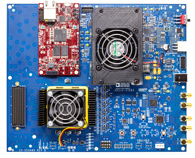
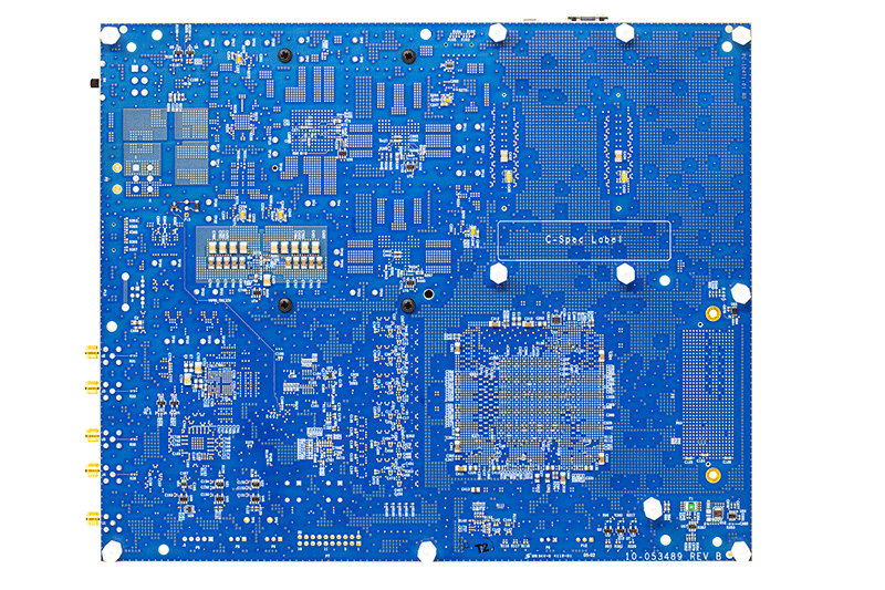
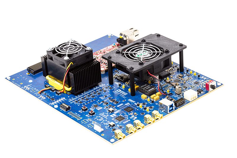
Open ToolEvaluation Kits
Latest Discussions
No discussions on AD9084 yet. Have something to say?
Start a Discussion on EngineerZone®