AD9739A
RECOMMENDED FOR NEW DESIGNS14-Bit, 2.5 GSPS, RF Digital-to-Analog Converter
- Part Models
- 2
- 1ku List Price
- Starting From $56.10
Part Details
- Direct RF synthesis at 2.5 GSPS update rate
- DC to 1.25 GHz in baseband mode
- 1.25 GHz to 3.0 GHz in mix-mode
- Industry leading single/multicarrier IF or RF synthesis
- Dual-port LVDS data interface
- Up to 1.25 GSPS operation
- Source synchronous DDR clocking
- Pin compatible with the AD9739
- Programmable output current: 8.7 mA to 31.7 mA
- Low power: 1.1 W at 2.5 GSPS
The AD9737A/AD9739A are 11-bit and 14-bit, 2.5 GSPS high performance RF DACs that are capable of synthesizing wideband signals from dc up to 3 GHz. The AD9737A/AD9739A are pin and functionally compatible with the AD9739 with the exception that the AD9737A/AD9739A do not support synchronization or RZ mode, and are specified to operate between 1.6 GSPS and 2.5 GSPS.
By elimination of the synchronization circuitry, some nonideal artifacts such as images and discrete clock spurs remain stationary on the AD9737A/AD9739A between power-up cycles, thus allowing for possible system calibration. AC linearity and noise performance remain the same between the AD9739 and the AD9737A/AD9739A.
The inclusion of on-chip controllers simplifies system integration. A dual-port, source synchronous, LVDS interface simplifies the digital interface with existing FGPA/ASIC technology. On-chip controllers are used to manage external and internal clock domain variations over temperature to ensure reliable data transfer from the host to the DAC core. A serial peripheral interface (SPI) is used for device configuration as well as readback of status registers.
The AD9737A/AD9739A are manufactured on a 0.18 µm CMOS process and operate from 1.8 V and 3.3 V supplies. They are supplied in a 160-ball chip scale ball grid array for reduced package parasitics.
Product Highlights
- Ability to synthesize high quality wideband signals with bandwidths of up to 1.25 GHz in the first or second Nyquist zone.
- A proprietary quad-switch DAC architecture provides exceptional ac linearity performance while enabling mixmode operation.
- A dual-port, double data rate, LVDS interface supports the maximum conversion rate of 2500 MSPS.
- On-chip controllers manage external and internal clock domain skews.
- Programmable differential current output with an 8.66 mA to 31.66 mA range.
Applications
- Broadband communications systems
- DOCSIS CMTS systems
- Military jammers
- Instrumentation, automatic test equipment
- Radar, avionics
Documentation
Data Sheet 1
User Guide 1
Technical Articles 1
3rd Party Solutions 1
Solutions Bulletin & Brochure 1
Device Drivers 2
ADI has always placed the highest emphasis on delivering products that meet the maximum levels of quality and reliability. We achieve this by incorporating quality and reliability checks in every scope of product and process design, and in the manufacturing process as well. "Zero defects" for shipped products is always our goal. View our quality and reliability program and certifications for more information.
| Part Model | Pin/Package Drawing | Documentation | CAD Symbols, Footprints, and 3D Models |
|---|---|---|---|
| AD9739ABBCZ | 160-Ball CSPBGA (12mm x 12mm x 1.4mm) | ||
| AD9739ABBCZRL | 160-Ball CSPBGA (12mm x 12mm x 1.4mm) |
| Part Models | Product Lifecycle | PCN |
|---|---|---|
|
Feb 11, 2015 - 14_0254 Bump and Assembly Transfer of Select 10x10 and 12x12 Flip Chip Products |
||
| AD9739ABBCZ | PRODUCTION | |
| AD9739ABBCZRL | PRODUCTION | |
This is the most up-to-date revision of the Data Sheet.
Software Resources
Evaluation Software 1
ACE Evaluation Software
Run this executable to install ACE on your computer to evaluate the AD9739A and AD9737A high-speed DACs.
Can't find the software or driver you need?
Hardware Ecosystem
| Parts | Product Life Cycle | Description |
|---|---|---|
| Fanout Buffers & Splitters 2 | ||
| ADCLK914 | RECOMMENDED FOR NEW DESIGNS | Ultrafast, SiGe, Open-Collector HVDS Clock/Data Buffer |
| ADCLK946 | RECOMMENDED FOR NEW DESIGNS | Six LVPECL Outputs, SiGe Clock Fanout Buffer |
| PLL Synthesizers 2 | ||
| ADF4350 | PRODUCTION | Wideband Synthesizer with Integrated VCO |
| ADF4150 | RECOMMENDED FOR NEW DESIGNS | Fractional-N/Integer-N PLL Synthesizer |
Tools & Simulations
LTspice® is a powerful, fast and free simulation software, schematic capture and waveform viewer with enhancements and models for improving the simulation of analog circuits.
Evaluation Kits
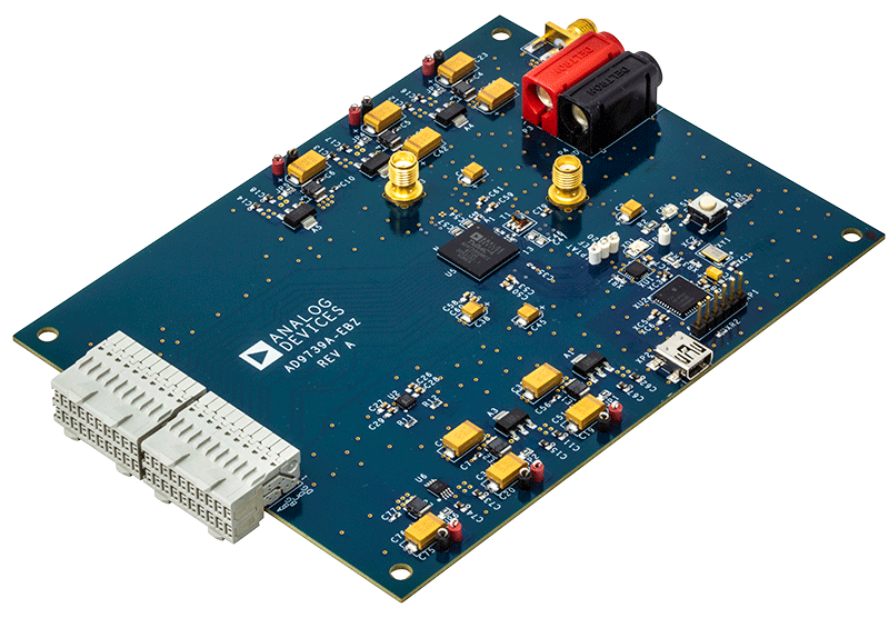
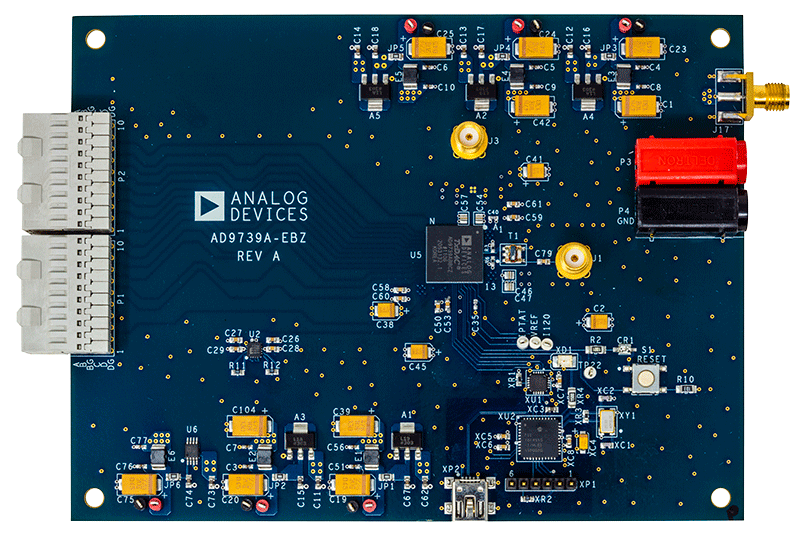

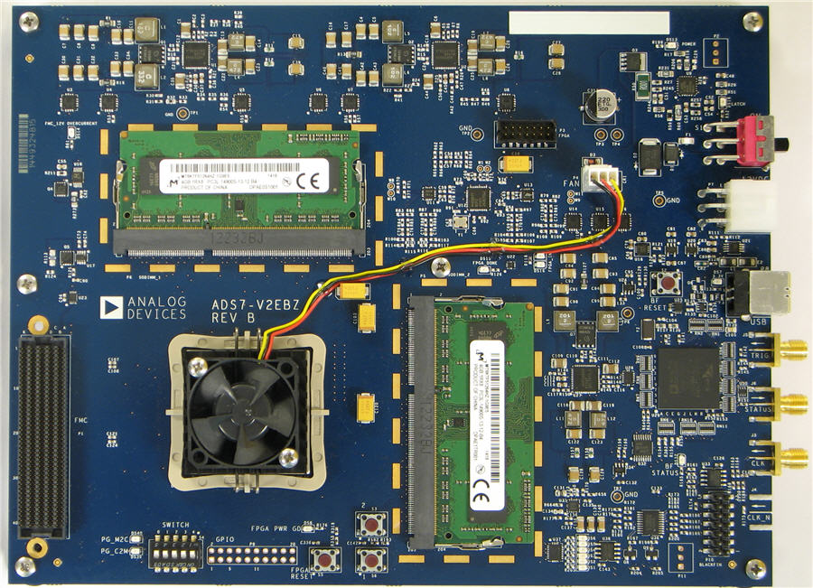
AD9739A Evaluation Board
Resources
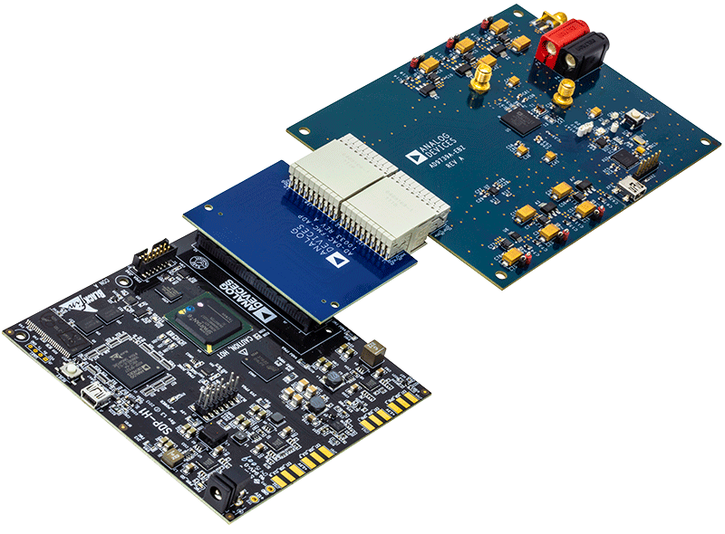
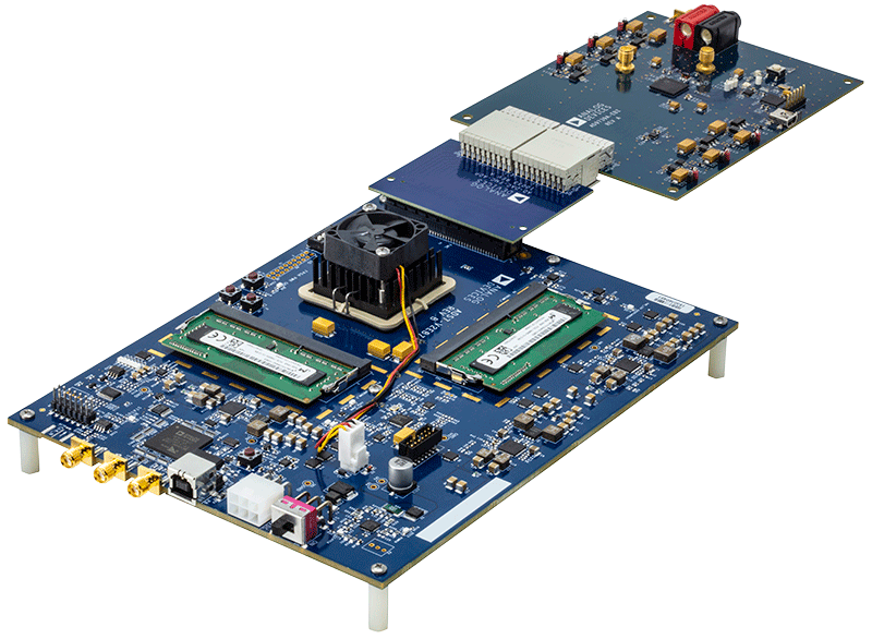
FPGA Based Data Capture Kit
Resources
Latest Discussions
No discussions on AD9739A yet. Have something to say?
Start a Discussion on EngineerZone®