Abstract
The common footprint strategy addresses requests from customers to have multiple sources for all parts in the BOM of voltage regulators, including controllers, power stages, and magnetics. However, rather than engaging in solely price-based competition as the distinguishing factor, Analog Devices has developed a coupled inductor IP that significantly enhances system performance, thereby providing customers with considerably higher system value.
Introduction
Many applications in data centers, artificial intelligence (AI), and communications use multiphase buck regulators with a 12 V input voltage. Figure 1(a) shows a conventional 8-phase buck with discrete inductors (DLs) placed in a row with an industrytypical 8.3 mm/phase pitch. The alternative solution on the very same layout is shown in Figure 1(b), where the discrete magnetics are replaced with two 4-phase coupled inductors (CLs).


The important questions are why customers would consider this alternative, and what are the incentives for ADI to develop a custom and unique solution, apart from just being different. The answer is in a significantly increased figure-of-merit (FOM) for the CL, which generally can be traded toward very different customer priorities. The common footprint (CF) strategy implies the same footprints for everything. So when the solution size is the same, the focus of optimization will be efficiency improvements.
Consider the fundamentals and related differentiation between DL and CL. The current ripple in each phase of the conventional buck can be found in Equation 1, where the duty cycle is D = VO/VIN, Vo is the output voltage, VIN is the input voltage, L is the inductance value, and Fs is the switching frequency.

Alternatively, the coupled inductor with a leakage inductance, Lk, and the mutual inductance, Lm, has the current ripple that can be shown as Equation 2.1 The FOM is expressed in Equation 3, where Nph is the number of coupled phases, ρ is a coupling coefficient (Equation 4), and j is a running index that defines an applicable interval of the duty cycle (Equation 5).


Comparing Equation 1 and Equation 2 shows the FOM is the differentiating factor that reflects the benefit of current ripple cancellation in CL vs. DL. The values of FOM depend on many factors, but it generally can reach significant numbers and imply a large performance improvement in case of CL. But the FOM advantage by itself does not ensure a big performance difference. The system must be designed to purposely take advantage of the increased FOM, according to the desired priorities.
CL Optimization
Starting with a VIN = 12 V to VO = 1 V reference design where DL = 100 nH provides a baseline performance, the CL FOM for Nph = 4 building block is plotted for the several practically reasonable values of the coupling coefficient Lm/Lk, as shown in Figure 2. The red curve Lm/Lk = 0 represents FOM = 1 baseline for the discrete inductor. The objective here is to keep the same transient performance with the same output capacitance tank Co, so the same 100 nH value is chosen for the CL leakage. As shown in the article “Addressing Core Loss in Coupled Inductors”2 and the video “Coupled Inductor Basics and Benefits”1, and is clearly visible in Figure 2, the Lm value is ideally as high as possible to maximize the coupling coefficient Equation 4, which will lead to increased FOM. In a given size (h = 12 mm, phase pitch 8.3 mm/ph), a reasonable Lm = 260 nH was achieved with an extremely conservative Isat = 25 A, which relates to the allowed current unbalance between phases. Notice that the load capability of CL is defined by Isat for Lk, which is >100 A per phase (at 105°C) in this CL design that exceeds the DL Isat rating.


The 12 V to 1 V application corresponds to the duty cycle range around D~0.083. For the conservative Lm/Lk = 2.6, FOM > 2.5 in Figure 2 suggests that Fs in CL can be comfortably dropped by 2× to keep the current ripple down. This should provide significant efficiency improvement, as several losses proportional to the switching frequency will decrease.
Increasing Lm is generally beneficial for the current ripple reduction, but Figure 3 suggests that Lm = 260 nH enables most of the current ripple cancellation benefit without going into diminishing returns where further Lm increases result in very limited improvement.


The corresponding current ripple is plotted in Figure 4, comparing the baseline design DL = 100 nH at Fs = 800 kHz with a proposed four phase CL = 4× 100 nH (Lm = 260 nH) with VIN = 12 V. Clearly, the CL solution can operate at Fs = 400 kHz instead of 800 kHz and still have a smaller current ripple as compared to DL = 100 nH at 800 kHz. The smaller peak to peak ripple implies that the rms of all circuit waveforms will be smaller as well, containing the conduction losses. The main efficiency improvement will come from the 2× reduction in Fs, which implies a big reduction in the switching losses, dead time loss in the body diodes of FETs, reverse recovery, gate drive losses, etc. Notice that the most significant efficiency improvement will appear at light load, where the AC losses are more visible. However, some losses, such as voltage and current overlap during the switching transitions, are proportional to the load current so the efficiency improvement will be visible at full load as well.


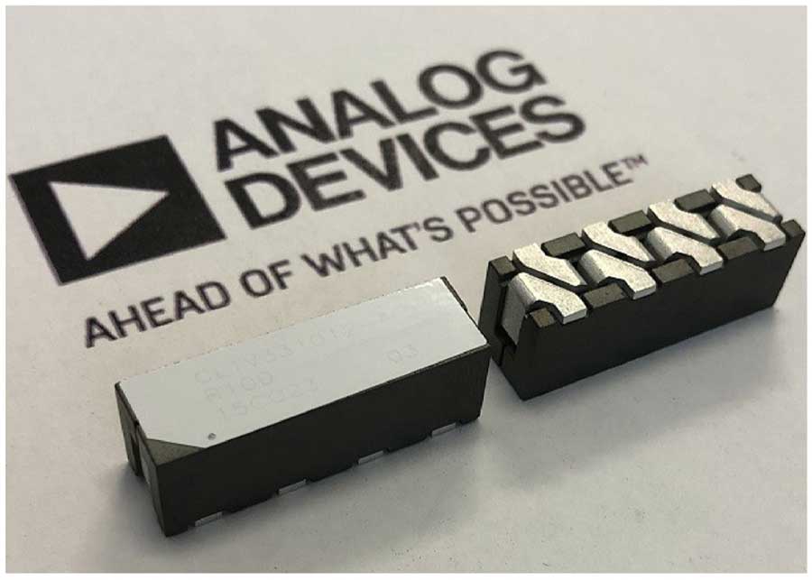
The developed 4× 100 nH coupled inductor is shown in Figure 5. Notice the lead arrangement that complies with the DL footprint for the multiple sources and alternatives.

Experimental Results
The transient performance of the four-phase buck is shown in Figure 6, comparing the waveforms of the 8-phase DL = 100 nH (600 kHz) and 2× CL = 4× 100 nH (400 kHz). The same current slew rate and the same output capacitance led to a similar transient performance, as expected. Potential reduction of the feedback bandwidth due to the reduction in the switching frequency for the CL is mitigated by multiphase topology as well as the fact that coupled phases effectively increase the phase margin of the feedback loop because transient change of the duty cycle in one phase results in all phase currents changing at the same time.


The corresponding efficiency comparison at different switching frequencies is shown in Figure 7, with dashed curves for DL and solid curves for CL. At a high switching frequency, the current ripple is insignificant for both CL and DL and therefore efficiency performance is similar. But because CL has a significant current ripple advantage, lowering the Fs for CL leads to a large reduction in the overall losses without much of an impact from the increased current ripple. The efficiency of the DL solution also improves with lower Fs, but with an increasingly slower pace as the outsized current ripple makes the rms of the waveforms worse and causes a nonlinear increase in core loss and ACR loss. This results in a significant efficiency advantage of CL vs. DL: 1% at peak and 0.5% at full load. The related thermal performance is improved as well.


Conclusion
According to the common footprint (CF) strategy, the CL solution to replace discrete inductors was designed in the identical footprint and the same overall size as a 4-phase building block for 12 V to ~1 V applications. The CL benefit was used to achieve a significant efficiency improvement, while the transient performance was preserved. Experimental results confirm the FOM-based design and optimization strategy.
The achieved overall performance improvement illustrates the advantages of the ADI IP on coupled inductors.
References
1 Alexandr Ikriannikov. “Coupled Inductor Basics and Benefits.” Maxim Integrated, August 2021.
2 Alexandr Ikriannikov and Di Yao. “Addressing Core Loss in Coupled Inductors.” Electronic Design News, December 2016.
Schultz, Aaron M. and Charles R. Sullivan. “Voltage Converter with Coupled Inductive Windings, and Associated Methods.” U.S. Patent 6,362,986, March 2001.
Li, Jieli. “Coupled Inductor Design in DC-DC Converters.” M.S. thesis, Dartmouth College, 2002.
Wong, Pit-Leong, Peng Xu, Bo Yang, and Fred C. Lee. “Performance Improvements of Interleaving VRMs with Coupling Inductors.” IEEE Transactions on Power Electronics, Vol. 16, No. 4, July 2001.
Dong, Yan. “Investigation of Multiphase Coupled-Inductor Buck Converters in Point-of-Load Applications.” Ph.D. thesis, Virginia Polytechnic Institute and State University, 2009.
Ikriannikov, Alexandr. “Coupled Inductor with Improved Leakage Inductance Control.” U.S. Patent 8,102,233, August 2009.
Ikriannikov, Alexandr. “Evolution and Comparison of Magnetics for the Multiphase DC-DC Applications.” Industry session at IEEE Applied Power Electronics Conference, March 2023.
Ikriannikov, Alexandr and Di Yao. “Converters with Multiphase Magnetics: TLVR vs. CL and the Novel Optimized Structure.” PCIM Europe 2023; International Exhibition and Conference for Power Electronics, Intelligent Motion, Renewable Energy and Energy Management, May 2023.
Ikriannikov, Alexandr and B. Xiao. “Generalized FOM for Multiphase Converters with Inductors.” IEEE Energy Conversion Congress and Exposition (ECCE), October 2023.