20A Constant Current Source/Battery Charger is 95% Efficient
20A Constant Current Source/Battery Charger is 95% Efficient
by
Goran Perica
Jun 1 1999
Introduction
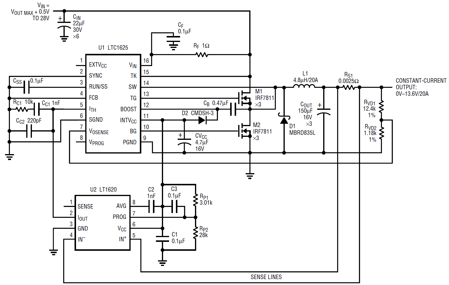
Generating precise, high DC currents presents a challenge due to the need for a current sensor that is sufficiently precise and low in cost and power dissipation. A current sense resistor is the most common type of current sensor. Current sense resistors can be very low in cost and are easy to use. Unfortunately, current sense resistors dissipate some power. Just how much power a current sense resistor will dissipate depends on the control circuit used for current sensing and the required precision of the output current. Another type of current sensor is based on Hall-effect devices. Although Hall-effect sensors meet the low power requirement, they are more difficult to use and are more expensive. Also, Hall-effect sensors have a limited bandwidth of 20kHz to 50kHz; as a result, a current regulator based on such a sensor has a slow transient response. As far as the cost and simplicity are concerned, current sense resistors are the better choice, as long as power dissipation is within the acceptable limits. The power dissipation in a current sense resistor depends on the current and the voltage across the resistor. Hence, keeping the voltage drop across the current sense resistor low is very important. The circuit in Figure 1 is a constant-current (CC), constant-voltage (CV) DC/DC converter that generates 20A of output current and maintains efficiency greater than 95% with a 24V input and 12.6V output.
Circuit Description
To achieve high efficiency, the circuit in Figure 1 employs the LTC1625 No RSENSE™ current mode DC/DC controller and LT1620 rail-to-rail current sense amplifier. The LTC1625 current mode controller does not require a current sense resistor to obtain the instantaneous current feedback for current mode operation. The instantaneous current value is obtained by sensing the voltage drop across power MOSFETs M1 and M2. Also, the LTC1625 provides overcurrent protection with current foldback that is based on the voltage drop across the MOSFETs. Unfortunately, the RDS(ON) of MOSFETs is a poorly controlled parameter that yields an overcurrent protection variation of more than 30%.

Figure 1. Constant-current (CC), constant-voltage (CV) DC/DC converter generates 20A of output current and maintains efficiency greater than 95% at a 24V input and 12.6V output.
The LT1620 achieves precise output current control. The minimum current limit of LTC1625 circuit must be set above the desired output current controlled by LT1620. The LT1620 current sense amplifier controls the LTC1625 via the ITH control pin. When the LT1620 does not pull down on the LTC1625’s ITH pin, the circuit operates in constant voltage (CV) mode.
Constant-Voltage Operation
When the output of the circuit in Figure 1 is left open or the load draws less than the programmed output current, the circuit operates in constant voltage mode (CV). In this condition, the LT1620 does not control the feedback loop. For a load current of less than 20A, the output voltage is set to the value controlled by output voltage divider RVD1 and RVD2. In the case of the circuit in Figure 1, the open-circuit output voltage is set to 13.6V, which is adequate for charging lead-acid batteries at room temperature. This voltage should have temperature compensation if the batteries are exposed to wide temperature variations. Temperature compensation is beyond the scope of this article—see AN51, Figure 16 for a simple compensation scheme, or consult the battery manufacturer for information.
Constant-Current Operation
The output current is set by the voltage (VPROG) across the resistor RP1 and by the value of output current sense resistor RS1. The LT1620 has a current sense amplifier with a gain of 10, which sets the actual current sense voltage to VPROG/10. Therefore, the output current (IOUT) will be:

where RS1 is the value of the output current sense resistor.
To obtain the highest possible precision, resistor RS1 should have separate voltage sense terminals (Kelvin, 4-terminal). The circuit in Figure 1 has VPROG set to 0.5V, resulting in 50mV of sense voltage across RS1 at the constant-current threshold. The resulting power dissipation in resistor RS1 at 20A of output current is only 1W. If the circuit in Figure 1 is used as a 12V, 20A battery charger, the efficiency loss in RS1 is only 0.4%.
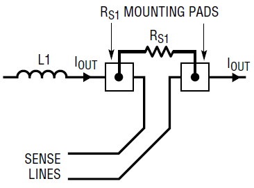
If a 2-terminal resistor is used, attention should be paid to connecting the current sense amplifier inputs (IN– and IN+) as close to the body of RS1 as possible. Connect the sense lines to the RS1 mounting pads as shown in Figure 2. By connecting the sense lines on the opposite sides of the output current flow (IOUT) as shown, the current sense error will be minimized. In any case, some error will result from using 2-terminal resistors for RS1. The output current error can be further minimized by increasing the program voltage, VPROG, by an amount proportional to the increase of resistance RS1 due to termination resistance of RS1. Because the value of RS1 is on the order of a few mΩ, termination resistance may be affected by such things as the type of solder used, size of component mounting holes, amount of copper on the PCB and whether the sense pins are connected on the side of RS1 or on the opposite side of printed circuit board.

Figure 2. Detailed view of connection to RS1.
The circuit in Figure 1 can be extended to even higher currents. To achieve the higher output currents, more MOSFETs can be used in parallel. An additional PNP/NPN gate drive buffer is also recommended. Integrated MOSFET drivers are not recommended because of the time delays that prevent proper operation of the LTC1625.
PCB Layout
The LTC1625 relies on the RDS(ON) of MOSFETs M1 and M2 for overcurrent protection. Because MOSFET RDS(ON) is highly dependent on junction temperature, it is very important to keep the junction temperature as low as possible by selecting MOSFETs with low RDS(ON) values. This also improves efficiency due to lower voltage drops across M1 and M2. If surface mount MOSFETs are used (SO-8, D-Pak or D2-Pak), good thermal management is required.
Best results can be obtained by using a multilayer printed circuit board with one or two of the inner layers used for a solid ground plane and/or a solid VCC plane. These planes serve as heat spreaders. The solid inner planes (GND, VCC or both) should be right next to the PCB layer where the MOSFETs are mounted. The thermal resistance between the MOSFETs package and solid inner plane depends on the distance between the two layers. Minimizing the distance between the heat spreading layer and the layer on which the MOSFETs are mounted will ensure the smallest temperature rise due to heat dissipation in the MOSFETs.
Conclusion
The circuit in Figure 1 presents a simple and efficient solution for battery charging and other applications requiring constant-current DC output. The new LTC1625 current mode controller makes it possible to achieve high output currents while maintaining high efficiency, due to its novel approach of sensing the voltage dropped across the on-resistance of the switching MOSFETs. The addition of the LT1620 as the output current controller allows the circuit to achieve high output-current precision.
