Precision half- and full-wave rectifiers are traditionally built using carefully selected components, including high speed op amps, fast diodes, and precision resistors. The high component count makes this solution expensive, and it suffers from crossover distortion and temperature drift variation between components.
This article shows how a dual-channel difference amplifier can be configured—with no external components—to provide a precision absolute value output. This innovative approach can achieve better precision, lower cost, and lower power consumption than conventional approaches.
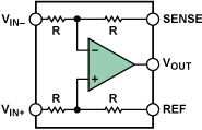
A difference amplifier1 comprises an op amp and four resistors configured as a subtractor, as shown in Figure 1. Featuring laser-wafer-trimmed resistors, low-cost monolithic difference amplifiers offer very high gain accuracy, low offsets, low offset drift, high common-mode rejection, and better overall performance than discrete alternatives.
Traditional Absolute Value Circuit
Figure 2 shows a schematic of a commonly used full-wave rectifier circuit. To achieve high performance, this design relies on two fast op amps and five precision resistors. When the input signal is positive, the output of A1 is negative, so D1 is reverse biased. D2 is forward biased, closing the feedback loop around A1 through R2 and forming an inverting amplifier. A2 sums the output of A1 times a gain of −2 with the input signal times a gain of −1, leaving a net gain of +1. When the input signal is negative, D1 is forward biased, closing the feedback loop around A1. D2 is reverse biased and does not conduct. A2 inverts the input signal, resulting in a positive output. Thus, the output of A2 is a positive voltage that represents the absolute value of the input, whether positive or negative.
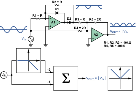
This design has several inherent performance and system shortcomings, including cost, crossover distortion, gain error, and noise. The design requires dual power supplies and many high performance components, further increasing the cost and complexity. The response time can be long because A1's output has to swing from –VBE to +VBE as the input signal crosses from 0 V + ΔV to 0 V – ∆V. High speed op amps and diodes can help mitigate this problem, but only at the cost of increased power dissipation. The gain accuracy of the absolute value output is determined by the matching of R1, R2, R3, R4, and R5. A substantial error between the positive and negative absolute value peaks will occur if even a single resistor is mismatched by a small amount. The overall noise gain is 6, amplifying the effects of op-amp noise, offset, and drift.
Improved Absolute Value Circuit
Figure 3 shows a simpler, more effective absolute value circuit that requires only one AD82774 dual-channel difference amplifier and a single positive supply. When the input signal is positive, A1 acts as a voltage follower. Both inputs of A2 are at the same potential as the input signal, so A2 simply passes the positive signal to the output. When the input signal is negative, the output of A1 is at 0 V, and A2 inverts the input signal. The overall result is the absolute value of the input signal. Signals as large as ±10 V can be rectified at frequencies as high as 10 kHz. If the signal to be rectified is very small, a pull-down resistor at each op amp output can improve the circuit performance around 0 V.

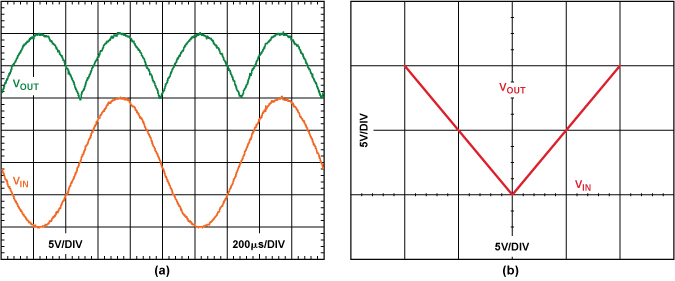
The function of this circuit, while deceptively simple, is possible only because of the AD8277's exceptional input and output characteristics and its ability to operate on a single supply. Unlike most op amps running on a single supply, the inputs of the difference amplifier can be driven below 0 V. This allows the inputs of A1 to accept a negative input signal while maintaining a 0 V output. Integrated ESD diodes at the inputs provide additional robust overvoltage protection. Figure 4 shows the input and output waveform and characteristic with a 20-V p-p input signal at 1 kHz.
This improved absolute value circuit overcomes many of the limitations of the conventional rectifier design and offers unexpected value. Most remarkable is the reduced number of required components: only a single device is needed. Eliminating the external diodes also eliminates the crossover distortion. The laser-wafer-trimmed resistors are precisely matched, guaranteeing gain error of less than 0.02%. The circuit's noise gain is only 2, resulting in lower noise and lower offset and drift. Operating on a single 2-V to 36-V supply, the AD8277 consumes less than 400 μA of quiescent current.
Conclusion
A precision full-wave rectifier built with a single dual-channel difference amplifier offers several advantages over traditional designs. Notably, the need for high performance external components and dual power supplies is eliminated, drastically lowering cost and reducing complexity. The difference amplifier solution has no crossover recovery problem and is optimized for low drift over a wide temperature range. Using the AD8277, a high precision absolute value circuit can be realized at low power consumption and low cost using a single IC.
参考資料
1http://www.analog.com/en/products/amplifiers/specialty-amplifiers/difference-amplifiers.html.
2http://sound.westhost.com/appnotes/an001.htm.
3Sedra, A.S. and K.C. Smith. Microelectronics Circuits. 4th ed. New York: Oxford University Press. 1998.
4http://www.analog.com/en/products/amplifiers/specialty-amplifiers/difference-amplifiers/ad8277.html.