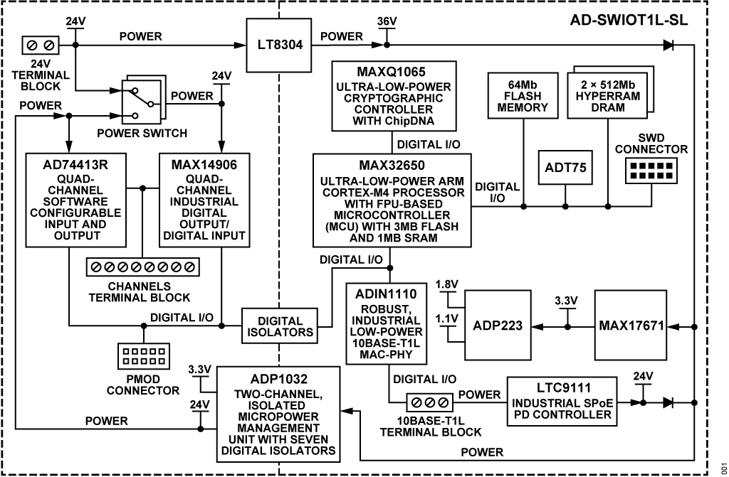
MAX32650
量产超低功耗Arm Cortex-M4 FPU微控制器,用于电池供电应用
DARWIN系列UP微控制器让小容量电池支持大型应用
- 产品模型
- 3
产品详情
- 超高效微控制器,用于电池供电应用
- 120MHz Arm Cortex-M4 FPU,工作在1.1V
- SmartDMA提供后台存储器传输,带可编程数据处理
- 120MHz高速和60MHz低功耗振荡器
- 7.3728MHz低功耗振荡器
- 32.768kHz和RTC时钟(要求外部晶振)
- 8kHz常电工作、超低功耗振荡器
- 3MB内部闪存
- 1MB内部SRAM
- 从缓存执行,104µA/MHz @ 1.1V
- 5种低功耗模式:工作、休眠、后台、深度休眠和备份
- 1.8V和3.3V I/O,无需电平转换器
- 可扩展、带缓存外部存储器接口:
- 120Mbps HyperBus/Xccela DDR2接口
- SPIXF用于外部闪存扩展,SPIXR用于外部SRAM扩展
- 240Mbps SDHC/eMMC/SDIO/microSD接口
- 最优外设组合,提高平台扩展性
- 16通道DMA
- 3个SPI主机(60MHz)/从机(48MHz)
- 1个QuadSPI主机(60MHz)/从机(48MHz)
- 多达3个4Mbaud UART,带流控制
- 2个1MHz I2C主机/从机
- I2S从机
- 四通道、7.8ksps、10位 Δ-Σ ADC
- USB 2.0高速设备接口,带PHY
- 16脉冲序列发生器
- 6个32位定时器,带8mA高驱动
- 1-Wire主机
- 2个看门狗定时器
- 信赖保护单元(TPU),用于IP/数据和安全
- 模运算加速器(MAA)、真随机数发生器(TRNG)
- 安全非易失密钥存储,SHA-256、AES-128/192/256
- 存储器解密完整性单元(MDIU)、安全引导ROM
DARWIN 是一种全新品类的低功耗微控制器,专为迅猛发展的物联网(IoT)而生。该器件的智能性令人难以置信,拥有业界最大的存储器,以及可大规模扩展的存储器架构。得益于可穿戴级电源技术,器件可永远运行。器件也非常坚固,足以抵御最高级的网络攻击。DARWIN微控制器可运行您能想到的任何应用 — 其他微控制器则望尘莫及。
UP系列微控制器非常适合目前先进的电池供电设备和无线传感器所要求的复杂程序。MAX32650—MAX32652为超低功耗、存储器可扩展微控制器,专门设计用于高性能、电池供电应用。器件基于Arm® Cortex®-M4,带浮点运算单元(FPU)、3MB闪存和1MB SRAM。支持存储器扩展,带多种存储器扩展接口,包括HyperBus™/Xccela™ DDR接口和两个SPI执行(SPIX)接口。安全数字接口支持外部高速存储卡,包括SD、SDIO、MMC、SDHC和microSD™。
齐全的电源管理特性提供5种低功耗模式提供可配置时钟、外设和电源管理方案。32KB、96KB或1024KB(全保持)的各个SRAM存储器组可置于一种既能降低功耗又能保留SRAM内容的模式。SmartDMA对传输的数据执行复杂的后台处理,包括从简单的算术运算到乘法/累积,而CPU保持关闭。这与传统DMA方案相比,能够大大降低总功耗。
MAX32651具有信赖保护单元(TPU),提供高级安全特性,例如模运算加速器(MAA,支持快速ECDSA)、AES引擎、TRNG、SHA-256散列算法以及安全装载程序。存储器解密完整性单元(MDIU)提供实时数据解密(纯文本或可执行),储存在外部闪存中。
MAX32652采用高密度、0.35mm焊球间距、140焊球WLP封装,目标为要求高I/O数量的微小尺寸产品。
应用
- 工业传感器、IoT
- 运动手表、健身监测器
- 可穿戴医疗贴片、便携式医疗设备
参考资料
视频 8


器件驱动器 1
模拟对话 1
ADI 始终高度重视提供符合最高质量和可靠性水平的产品。我们通过将质量和可靠性检查纳入产品和工艺设计的各个范围以及制造过程来实现这一目标。出货产品的“零缺陷”始终是我们的目标。查看我们的质量和可靠性计划和认证以了解更多信息。
| 产品型号 | 引脚/封装图-中文版 | 文档 | CAD 符号,脚注和 3D模型 |
|---|---|---|---|
| MAX32650GCE+ | 144-TQFP-20X20X1.0 | ||
| MAX32650GWQ+ | 96-WLCSP-N/A | ||
| MAX32650GWQ+T | 96-WLCSP-N/A |
| 产品型号 | 产品生命周期 | PCN |
|---|---|---|
|
5月 14, 2019 - 1957 DESIGN |
||
| MAX32650GCE+ | 量产 | |
| MAX32650GWQ+ | 量产 | |
这是最新版本的数据手册
软件资源
CodeFusion Studio™
CodeFusion Studio(CFS)是一个基于Microsoft Visual Studio(VS Code)的嵌入式软件开发平台。
更多内容Evaluation Software 1
找不到您所需的软件或驱动?
工具及仿真模型
评估套件
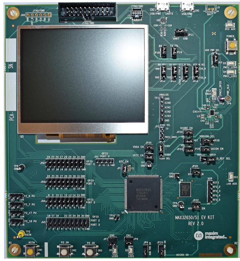
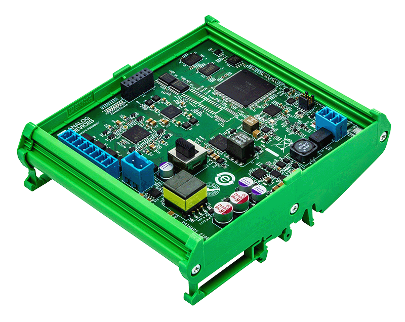
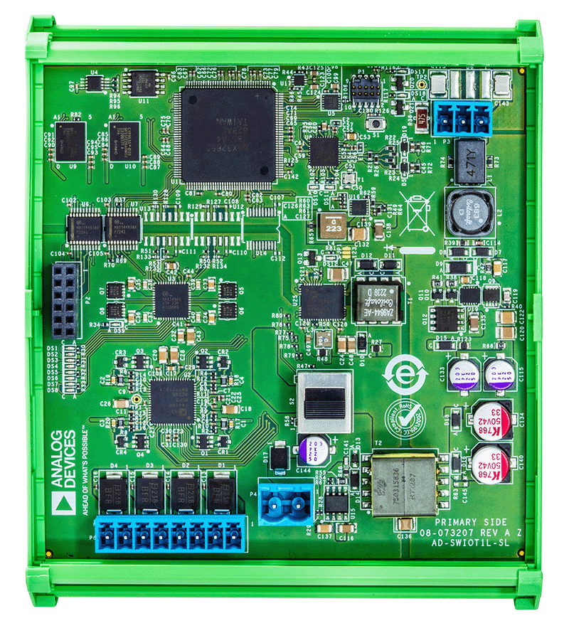
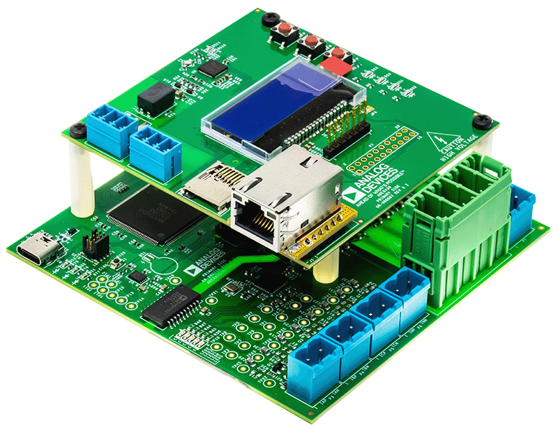
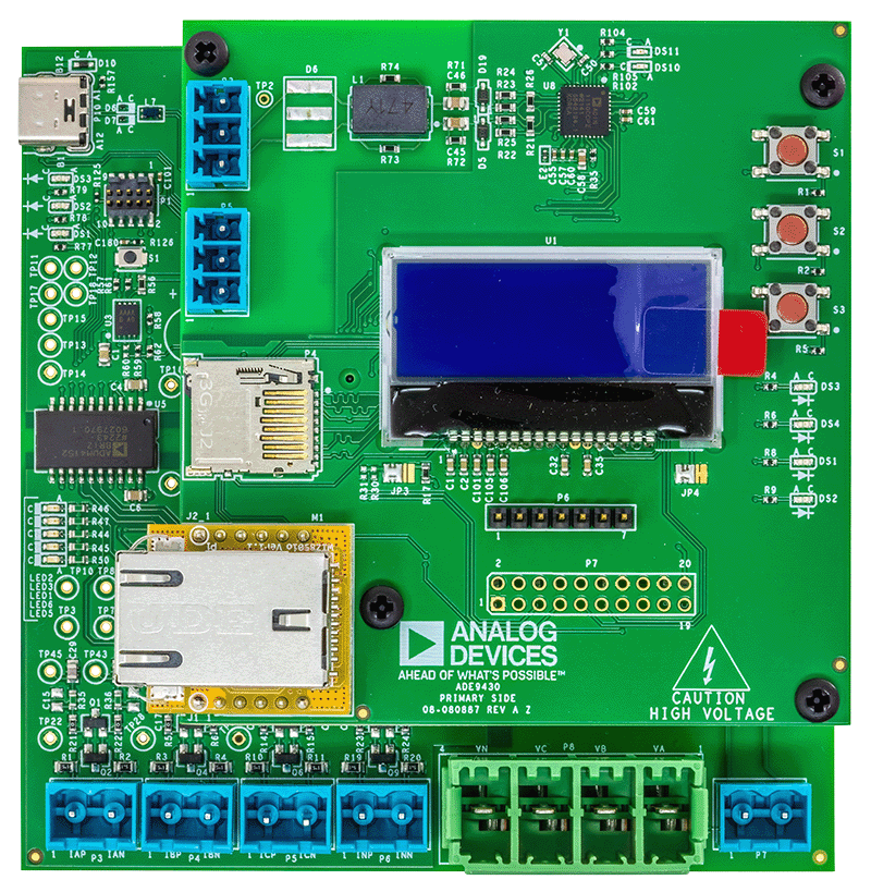
MAX32650/MAX32651/MAX32652评估板
特性和优点
- 3.5in 320 x 240彩色TFT显示屏
- 64MB HyperRAM
- 64MB XIP闪存
- 1MB XIP RAM
- USB 2.0 Micro B接口
- USB 2.0 Micro B至串行UART
- 利用跳线可选择UART0和UART2
- Micro SD卡接口
- 可通过0.1in连接头访问选择GPIO
- 通过0.1in连接头访问四个模拟输入
- Arm® 或SWD JTAG 20引脚连接头
- 板载PMIC为MAX32650供电
- 通过任一USB端口为电路板供电
- 通过跳线对全部IC电压轨进行各种测量
- 板载1.8V和3.3V稳压器,用于外设
- 2个通用LED和2个通用按键开关
产品详情
MAX32650评估板提供评估MAX32650超低功耗、存储器可扩展微控制器的平台,器件专门设计用于高性能电池供电应用。
使用MAX32650上的LCD控制器系列视频
 第1部分:到底什么是LCD控制器?
应用
- 工业传感器、IoT
- 运动手表、健身监测器
- 可穿戴医疗贴片、便携式医疗设备
资料
软件
MAX32650评估套件
软件

MAX32650/MAX32651/MAX32652评估板
特性和优点
- 3.5in 320 x 240彩色TFT显示屏
- 64MB HyperRAM
- 64MB XIP闪存
- 1MB XIP RAM
- USB 2.0 Micro B接口
- USB 2.0 Micro B至串行UART
- 利用跳线可选择UART0和UART2
- Micro SD卡接口
- 可通过0.1in连接头访问选择GPIO
- 通过0.1in连接头访问四个模拟输入
- Arm® 或SWD JTAG 20引脚连接头
- 板载PMIC为MAX32650供电
- 通过任一USB端口为电路板供电
- 通过跳线对全部IC电压轨进行各种测量
- 板载1.8V和3.3V稳压器,用于外设
- 2个通用LED和2个通用按键开关
产品详情
MAX32650评估板提供评估MAX32650超低功耗、存储器可扩展微控制器的平台,器件专门设计用于高性能电池供电应用。
使用MAX32650上的LCD控制器系列视频
第1部分:到底什么是LCD控制器?
应用
- 工业传感器、IoT
- 运动手表、健身监测器
- 可穿戴医疗贴片、便携式医疗设备
资料
软件
60 GHz Wireless Connector
资料
软件
具有 10BASE-T1L 评估和开发平台的软件可配置模拟和数字 I/O
资料
软件
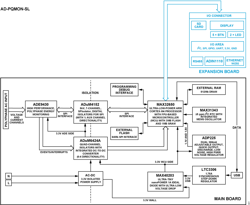
Power Quality Monitor Development Platform
资料
最新评论
需要发起讨论吗? 没有关于 MAX32650的相关讨论?是否需要发起讨论?
在EngineerZone®上发起讨论