GOLDSTANDARD-DONOTLAUNCH-REFERENCEDESIGN


概览
设计资源
器件驱动器
软件(如C代码和/或FPGA代码等)用于与元件的数字接口通信。
AD7280A GitHub no-OS Driver Source Code
AD7280A IIO Lithium Ion Battery Monitoring System GitHub Linux Driver Source Code
优势和特点
- Measure up to 48 battery channels
- 1.6mV Cell Voltage Accuracy
- Alarm interrupts for different voltage conditions
- Battery cell balancing for load sharing
- Lithium battery management system
电路功能与优势
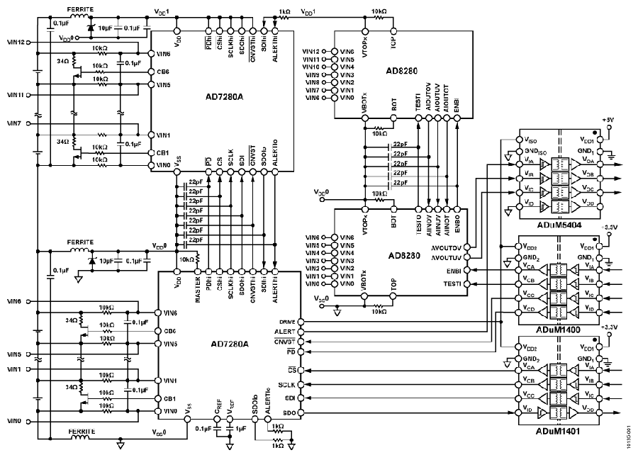
Lithium ion (Li-Ion) battery stacks contain a large number of individual cells that must be monitored correctly in order to enhance the battery efficiency, prolong the battery life, and ensure safety. The 6-channel
AD7280A devices in the circuit shown in Figure 1 act as the primary monitor providing accurate voltage measurement data to the System Demonstration Platform (SDP-B) evaluation board, and the 6-channel AD8280 devices act as the secondary monitor and protection system. Both devices can operate from a single wide supply range of 8 V to 30 V and operate over the industrial temperature range of −40°C to +105°C.The AD7280A contains an internal ±3 ppm reference that allows a cell voltage measurement accuracy of ±1.6 mV. The ADC resolution is 12 bits and allows conversion of up to 48 cells within 7 μs.
The AD7280A has cell balancing interface outputs designed to control external FET transistors to allow discharging of individual cells and forcing all the cells in the stack to have identical voltages.
The AD8280 functions independently of the primary monitor and provides alarm functions indicating out of tolerance conditions. It contains its own reference and LDO, both of which are powered completely from the battery cell stack. The reference, in conjunction with external resistor dividers, is used to establish trip points for the over/undervoltages. Each cell channel contains programmable deglitching (D/G) circuitry to avoid alarming from transient input levels.
The AD7280A and AD8280, which reside on the high voltage side of the battery management system (BMS) have a daisychain interface, which allows up to eight AD7280A’s and eight AD8280’s to be stacked together and allows for 48 Li-Ion cell voltages to be monitored. Adjacent AD7280A's and AD8280’s in the stack can communicate directly, passing data up and down the stack without the need for isolation.
The master devices on the bottom of the stack use the SPI
interface and GPIOs to communicate with the SDP-B
evaluation board, and it is only at this point that high voltage
galvanic isolation is required to protect the low voltage side of
the SDP-B board. The ADuM1400, ADuM1401 digital isolator, and the ADuM5404 isolator with integrated dc-to-dc converter
combine to provide the required eleven channels of isolation in
a compact and cost effective solution. The ADuM5404 also provides isolated 5 V to the VDRIVE input of the lower AD7280A and the VDD2 supply voltage for the ADuM1400 and ADuM1401 isolators.

电路描述
The AD8280 is a hardwire-only safety monitor for lithium ion battery stacks. In conjunction with the AD7280A, the AD8280 provides a low cost, redundant, battery backup monitor with adjustable threshold detection and shared or separate alarm outputs. It has a self-test feature, making it suitable for high reliability applications, such as automotive hybrid electric vehicles or higher voltage industrial usage, such as uninterruptible power supplies. Both the AD7280A and the AD8280 obtain power from the battery cells they monitor.
The ADuM5404 includes an integrated dc-to-dc converter,
which is used to power the high voltage side of the ADuM1400
and ADuM1401 isolators and provide the VDRIVE supply to
the AD7280A SPI interface. These 4-channel, magnetically
isolated circuits are a safe, reliable, and easy-to-use alternative
to optocouplers.
To optimize the performance of the daisy-chain communication
under noisy conditions, for example, when experiencing
electromagnetic interference, the daisy-chain signals are
shielded on an inner layer of the printed circuit board (PCB).
Shielding is provided above and below by a VSS supply plane,
which is connected to the VSS pin of the upper device in the
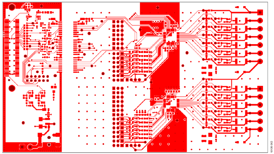
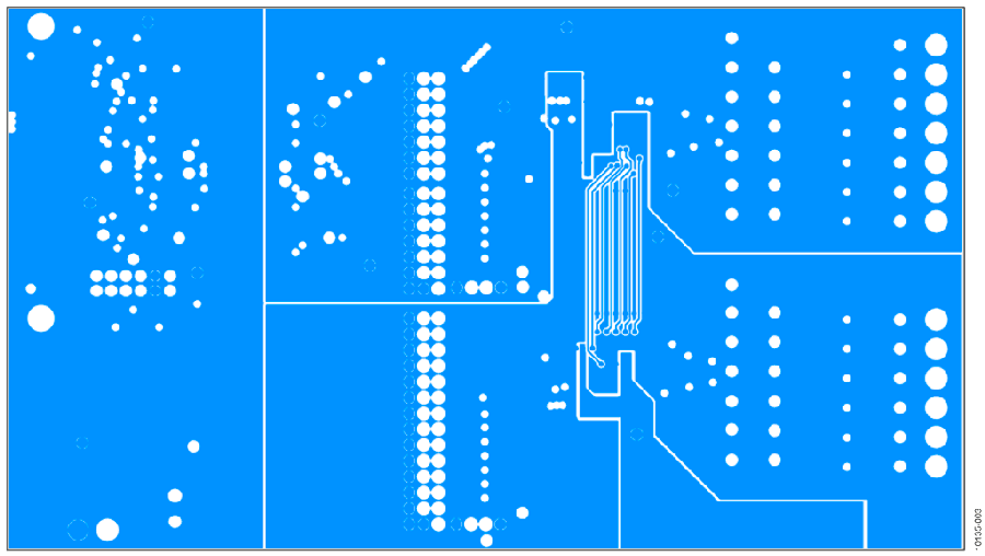
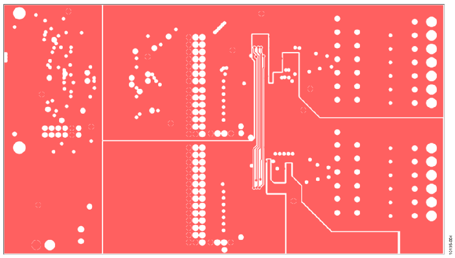
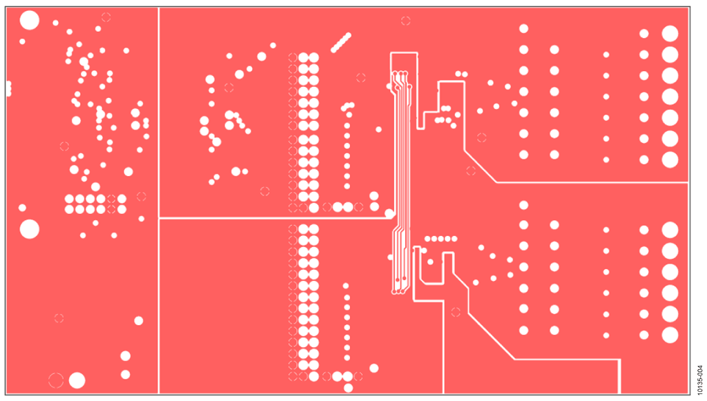
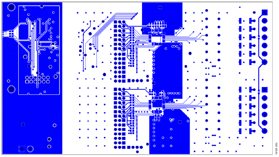
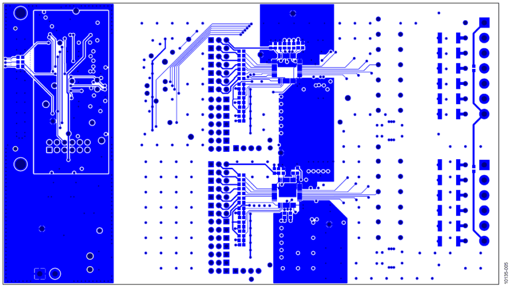
chain. Figure 2 shows the top layer of the EVAL-CN0235-SDPZ PCB, which contains the upper shielding for the AD7280A, and Figure 5 shows the bottom layer, which contains the upper
shielding for the AD8280. Figure 3 shows the inner layer
(layer 2), which contains the shielded daisy-chain signals, and
the shielding below is carried out on Layer 3 as shown in Figure 4.
Individual 22 pF capacitors are placed on each daisy-chain
connection and are terminated to either the VSS pin of the
upper device or the VDD pin of the lower device, depending on
the direction in which data is flowing on the daisy chain. The
PD, CS, SCLK, SDI, and CNVST daisy-chain connections pass
data up the chain, and the 22 pF capacitors on these pins are
terminated to the VSS of the upper device in the chain.


The SDOlo and ALERTlo daisy-chain connections pass data down the chain, and the 22 pF capacitors on these pins are terminated to the VDD of the lower device in the chain. A direct low impedance trace is used to connect the VDD of the lower device with the VSS of the upper device to hold the two potentials as close as possible together in a noisy environment.
A ground fence at the isolation barrier is used to enclose the low voltage side, which consists of the left hand side of the PCB. This fence consists of a guard ring laced together by vias and connects to the digital ground on all layers throughout the board. Noise on power and ground planes that reach the edge of the circuit board can radiate causing emissions, but with this shielded structure the noise is reflected back.
Input-to-output dipole radiation can also be generated when driving a current source across a gap between ground planes. To help minimize this, a continuous shield is used at the isolation gap whereby the ground planes are extended on all layers throughout the PCB to create a cross-barrier coupling using overlapping shields; and the isolation gap on each layer is kept to a minimum, with a gap of 0.008 inches used on the tested board. For further recommendations to control radiated emissions with isoPower® devices, such as the ADuM5404 used in this circuit, please refer to Application Note AN-0971.
Test Results
An important measure of the performance of the circuit is the
amount of noise in the final output voltage measurement.
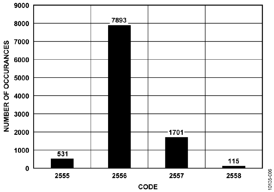
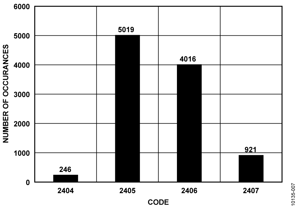
Figure 6 shows a histogram of 10,000 measurement samples taken for the VIN3−VIN2 channel. This data was taken with the CN0235 Evaluation Board connected to the EVAL-SDP-CB1Z System Demonstration Platform (SDP-B) evaluation board. Details of the setup are described in the Circuit Evaluation and Test section of this circuit note.
Twelve Li-Ion batteries were connected to the input screw terminals. Note that there are only a small percentage of codes that fall outside the primary bin due to noise. Figure 6 and Figure 7 show 3 LSBs peak-to-peak noise, corresponding to approximately 0.5 LSBs rms.
A complete design support package for this circuit note can be
found at www.analog.com/CN0235-DesignSupport.


常见变化
电路评估与测试
Equipment Needed
- PC with a USB port and Windows® XP or Windows Vista® (32-bit), or Windows® 7 (32-bit)
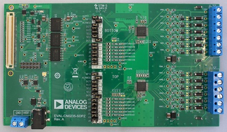
- EVAL-CN0235-SDPZ circuit evaluation board
- EVAL-SDP-CB1Z SDP-B evaluation board
- CN0235 SDP evaluation software
- Power supply: +6 V, or +6 V “wall wart”
- Li-Ion batteries or precision dc supply
Getting Started
Load the evaluation software by placing the CN0235 Evaluation Software disc in the CD drive of the PC. Using "My Computer," locate the drive that contains the evaluation software.
Functional Block Diagram
Setup
Test
Once USB communications are established, the SDP-B board can be used to send, receive, and capture serial data from the EVAL-CN0235-SDPZ board.
Information regarding the SDP-B board can be found in the
SDP-B User Guide.