LTC6951
LAST TIME BUYUltralow Jitter Multi-Output Clock Synthesizer with Integrated VCO
- Part Models
- 4
- 1ku List Price
- Starting From $10.84
Part Details
- Low Noise Integer-N PLL with Integrated VCO
- Output Jitter:
- 90fs RMS (12kHz to 20MHz)
- 115fs RMS (ADC SNR Method)
- Noise Floor = –165dBc/Hz at 250MHz
- EZSync™, ParallelSync™ Multichip Synchronization
- SYSREF Generation for JESD204B/JESD204C, Subclass 1
- Output Frequency Range:
- 1.95MHz to 2.5GHz (LTC6951)
- 2.1MHz to 2.7GHz (LTC6951-1)
- –229dBc/Hz Normalized In-Band Phase Noise Floor
- –277dBc/Hz Normalized In-Band 1/f Noise
- Five Independent, Low Noise Outputs
- Reference Input Frequency up to 425MHz
- LTC6951Wizard™ Software Design Tool Support
- –40°C to 105°C Operating Junction Temperature Range
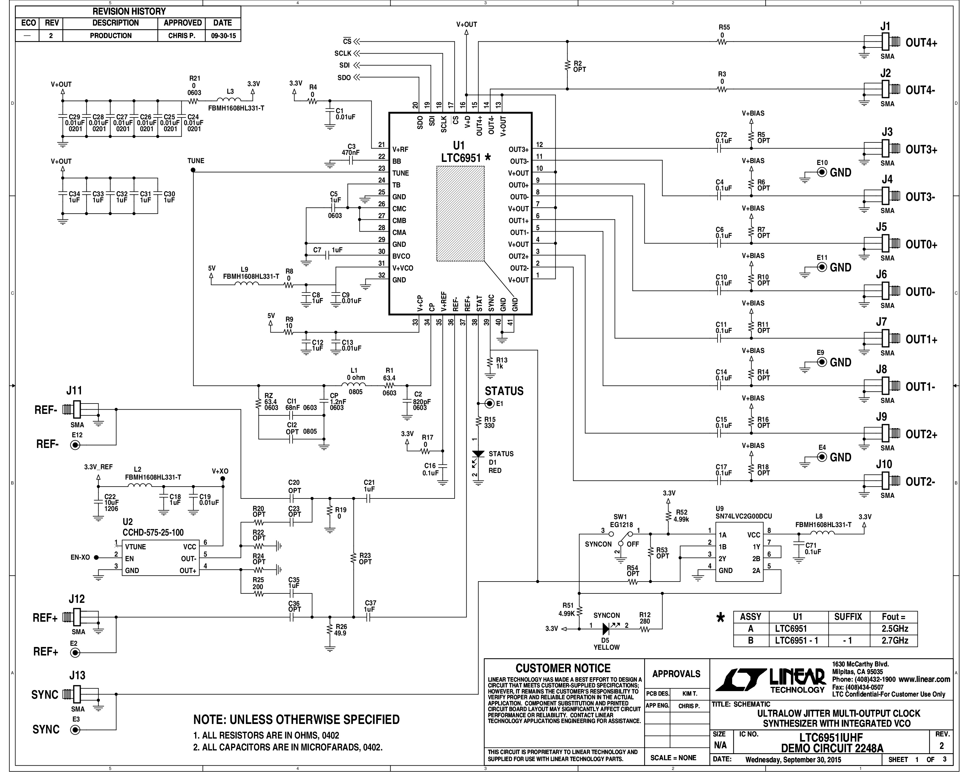
The LTC6951 is a high performance, low noise, Phase Locked Loop (PLL) with a fully integrated VCO. The low noise VCO uses no external components and is internally calibrated to the correct output frequency with no external system support.
The clock generation section provides five outputs based on the VCO prescaler signal with individual dividers for each output. Four outputs feature very low noise, low skew CML logic. The fifth output is low noise LVDS. All outputs can be synchronized and set to precise phase alignment using the programmable delays.
Choose the LTC6951-1 if any desired output frequency falls in the ranges 2.5GHz to 2.7GHz, 1.66GHz to 1.8GHz, or 1.25GHz to 1.35GHz. Choose the LTC6951 for all other frequencies.
Applications
- High Performance Data Converter Clocking
- Wireless Infrastructure
- Test and Measurement
Documentation
Data Sheet 1
User Guide 2
Application Note 2
Technical Articles 1
Product Selector Card 1
ADI has always placed the highest emphasis on delivering products that meet the maximum levels of quality and reliability. We achieve this by incorporating quality and reliability checks in every scope of product and process design, and in the manufacturing process as well. "Zero defects" for shipped products is always our goal. View our quality and reliability program and certifications for more information.
| Part Model | Pin/Package Drawing | Documentation | CAD Symbols, Footprints, and 3D Models |
|---|---|---|---|
| LTC6951IUHF#PBF | 40-Lead QFN (5mm x 7mm x 0.75mm w/ EP) | ||
| LTC6951IUHF#TRPBF | 40-Lead QFN (5mm x 7mm x 0.75mm w/ EP) | ||
| LTC6951IUHF-1#PBF | 40-Lead QFN (5mm x 7mm x 0.75mm w/ EP) | ||
| LTC6951IUHF-1#TRPBF | 40-Lead QFN (5mm x 7mm x 0.75mm w/ EP) |
This is the most up-to-date revision of the Data Sheet.
Software Resources
Can't find the software or driver you need?
Request a Driver/SoftwareHardware Ecosystem
| Parts | Product Life Cycle | Description |
|---|---|---|
| Analog to Digital Converters 2 | ||
| LTC2107 | PRODUCTION | 16-Bit, 210Msps High Performance ADC |
| LTC2123 | PRODUCTION | Dual 14-Bit 250Msps ADC with JESD204B Serial Outputs |
| Clocks 1 | ||
| LTC6953 | LAST TIME BUY | Ultralow Jitter, 4.5GHz Clock Distributor with 11 Outputs and JESD204B/JESD204C Support |
| Comparators 1 | ||
| LTC6957 | Low Phase Noise, Dual Output Buffer/Driver/Logic Converter | |
| Fanout Buffers & Splitters 1 | ||
| LTC6954 | LAST TIME BUY | Low Phase Noise, Triple Output Clock Distribution Divider/Driver |
| PLL Synthesizers 1 | ||
| ADF4002 | RECOMMENDED FOR NEW DESIGNS | Phase Detector / PLL Frequency Synthesizer |
Tools & Simulations
Linduino 3
IBIS Model 1
Design Tool 1
Linduino is Analog Devices’ Arduino compatible system for developing and distributing firmware libraries and example code for our integrated circuits. Each Linduino-supported product includes an example main program, defined in the LTSketchbook/Part Number folder and driver code, defined in the LTSketchbook/libraries folder.
Linduino code repository on GitHub and instructions on how to use the code.
Evaluation Kits
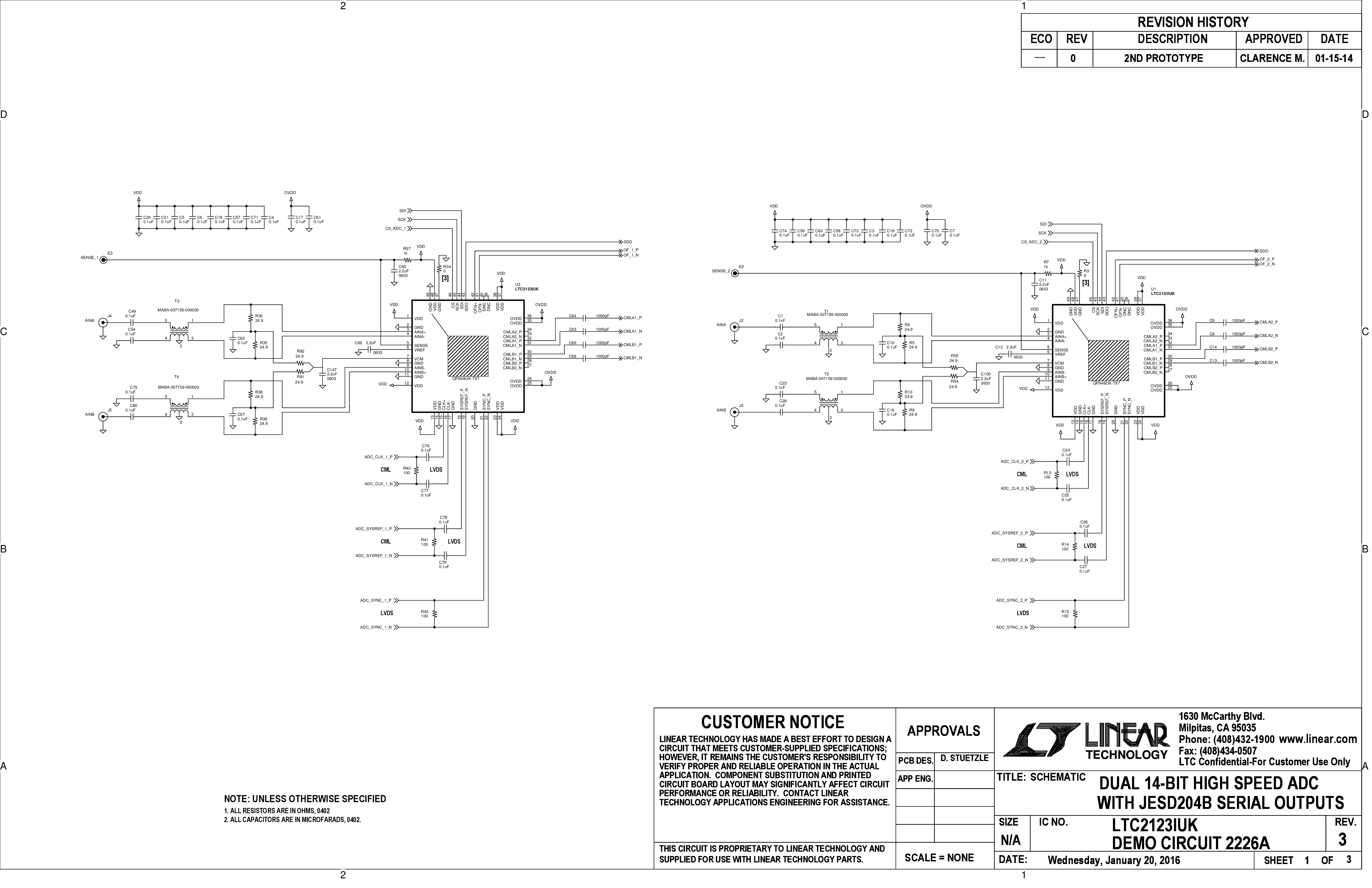
4-Channel 14-Bit 250Msps JESD204B ADC with Clocking [Featuring LTC2123, LTC6951]
Resources
Software
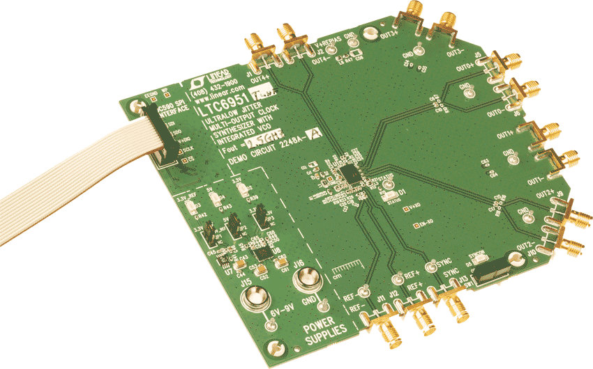
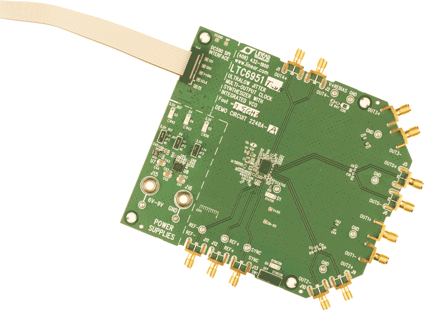
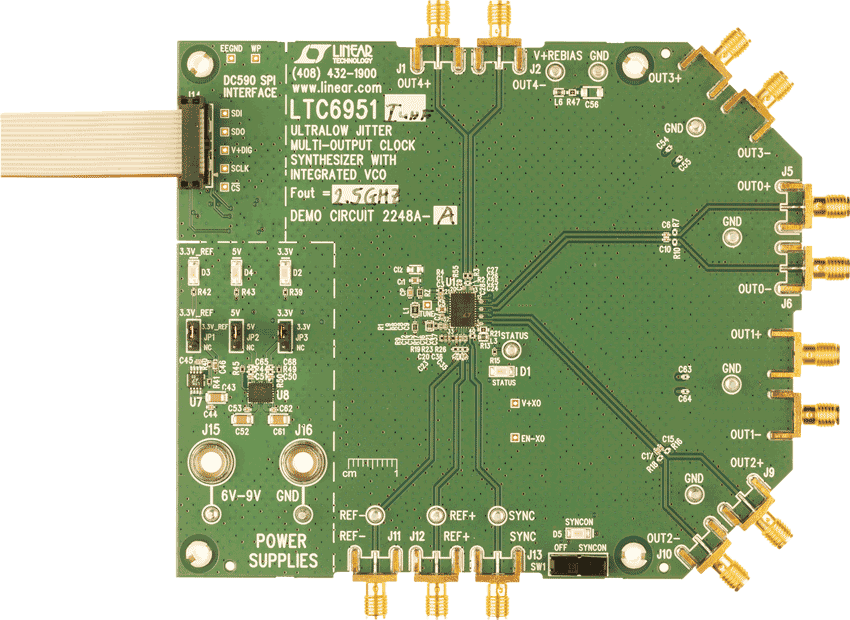
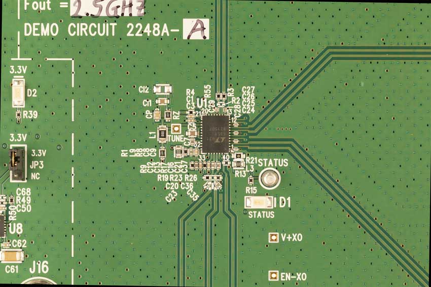
LTC6951 Demo Board | 5-Output Integer-N PLL with Integrated VCO, Output Range: 1.95MHz to 2.5GHz (requires DC590 or DC2026)
Resources
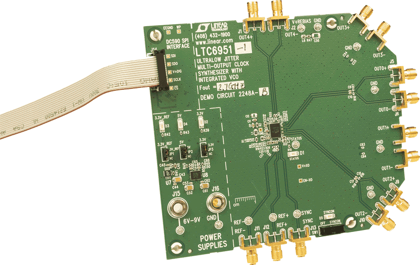
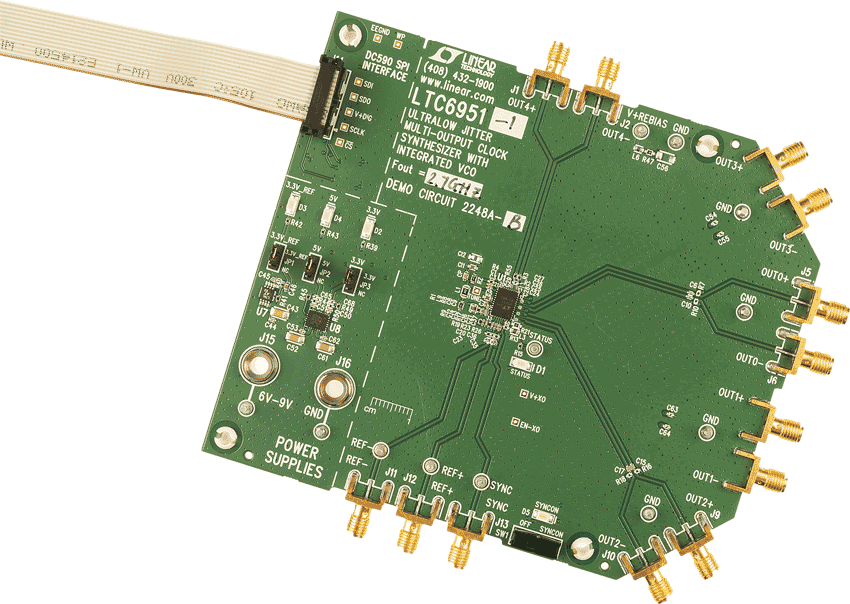
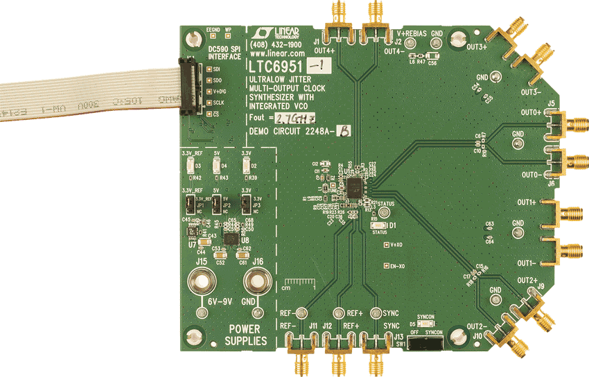
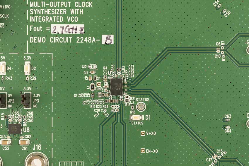
LTC6951-1 Demo Board | 5-Output Integer-N PLL with Integrated VCO, Output Range: 2.1MHz to 2.7GHz (requires DC590 or DC2026)
Resources
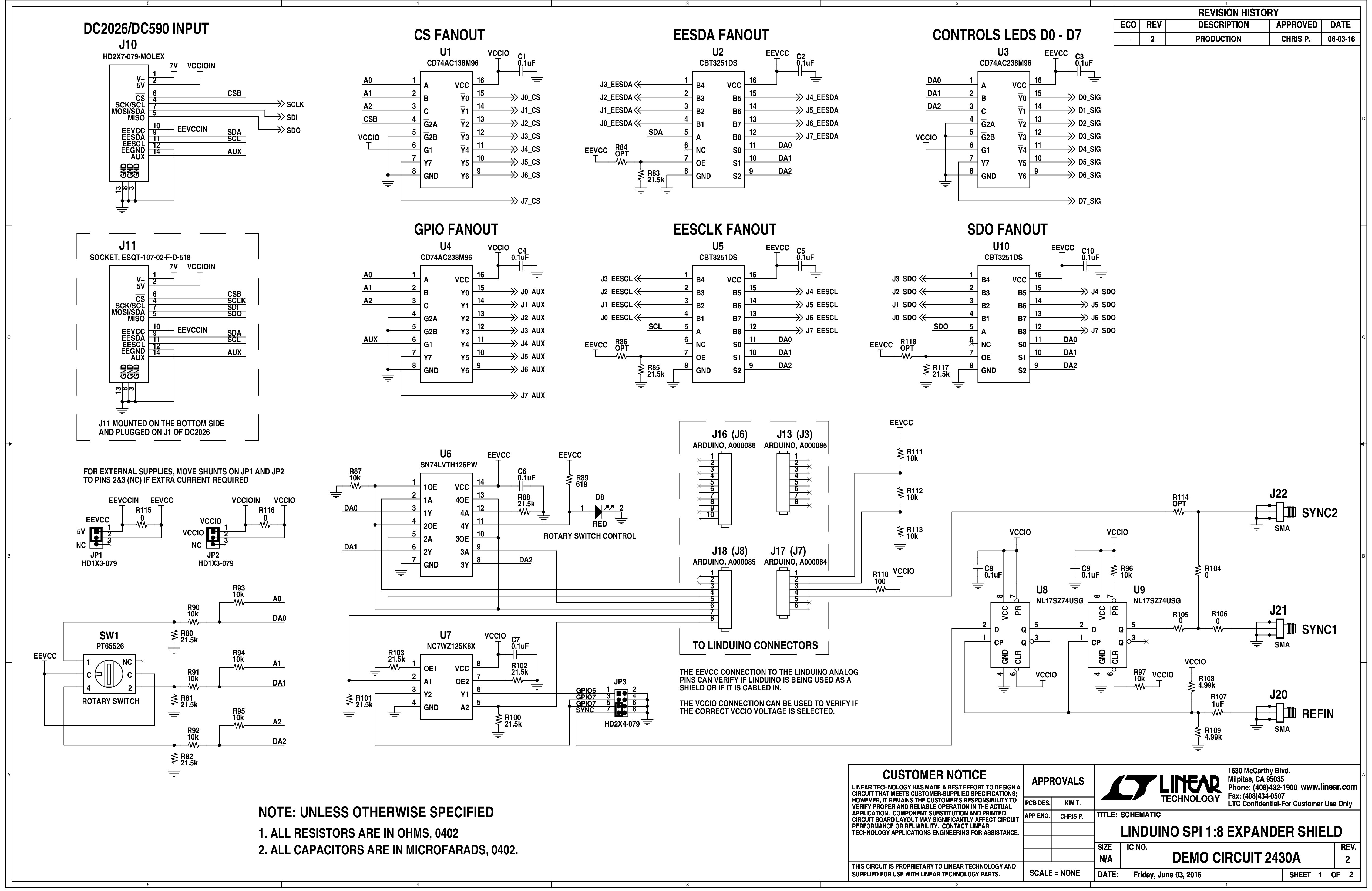
DC2430A Linduino SPI 1:8 Expander Demonstration Board (DC2026 Included)
Resources
Latest Discussions
No discussions on LTC6951 yet. Have something to say?
Start a Discussion on EngineerZone®