AD9084
预发布Apollo MxFE Quad, 16-Bit, 28 GSPS RF DAC and Quad, 12-Bit, 20 GSPS RF ADC
产品详情
- Flexible reconfigurable common platform design
- 4 DACs and 4 ADCs (4D4A)
- Usable RF Analog bandwidth up to 18 GHz
- Maximum DAC/ADC sample rate up to 28 GSPS/20 GSPS
- DAC to ADC sample rate ratios of 1 and 2
- Clocking
- On-chip PLL (7 GHz to 14 GHz)
- External RFCLK input up to 20 GHz
- Multichip synchronization via subclass1
- Single-ended (SE) or differential (DIFF) ADC inputs
- Two separate versions, both 50 Ω input impedance
- Single-ended version with on-chip wide bandwidth balun
- Differential ADC AC performance at 20 GSPS
- Full-scale input voltage: 500 mV p-p/−2 dBm
- Noise density: −150 dBFS/Hz at −20 dBFS at 2 GHz
- HD2/HD3: −65 dBFS/−70 dBFS at −7 dBFS at 2 GHz
- IMD3: −75 dBFS at – 13 dBFS/tone at 2 GHz
- DAC AC performance at 28 GSPS
- Full-scale output power: −2.1 dBm at 2 GHz
- IMD3: −75 dBc at – 13 dBFS/tone at 2 GHz to 10 GHz
- NSD (shuffling disabled): −164 dBFS/Hz at 0 dBFS at 2 GHz
- Versatile digital features
- Supports real or complex digital data (8-, 12-, 16-bit)
- Configurable DDC and DUC
- 8 fine complex DUCs and 4 coarse complex DUCs
- 8 fine complex DDCs and 4 coarse complex DDCs
- Option to bypass fine and coarse DUC/DDC
- DUC/DDC alias rejection
- 85 dB for interpolation filters
- 100 dB for decimation filters
- Fractional sample rate converter (FSRC)
- Programmable FIR filters for transmit/receive
- Multiple loopback (ADC to DAC) supported
- ~45 ns without DSP path
- Dynamic configuration through SPI/HSCI/GPIO
- Spectrum sniffer/monitor
- Interfaces
- SPI
- High-Speed Control Interface (HSCI)
- JESD204B/JESD204C: 20 Gbps/32.5 Gbps
- 24 lanes for Rx, 24 lanes for Tx
- Receive AGC support
- Fast detect with low latency for fast AGC control
- Signal monitor for slow AGC control
- Auxiliary features
- Power amplifier downstream protection circuitry
- On-chip temperature monitoring unit
- TDD power savings option
- Total power consumption range dependent on device configuration: 20 W to 30 W
- 24 mm × 26 mm, 899-ball BGA with 0.8 mm pitch
- Operating junction temperature (TJ): −40°C to +110°C
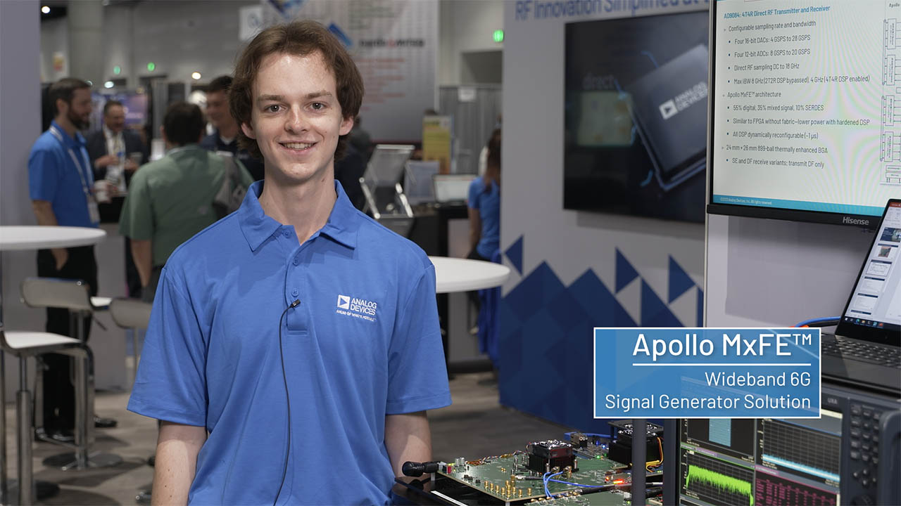
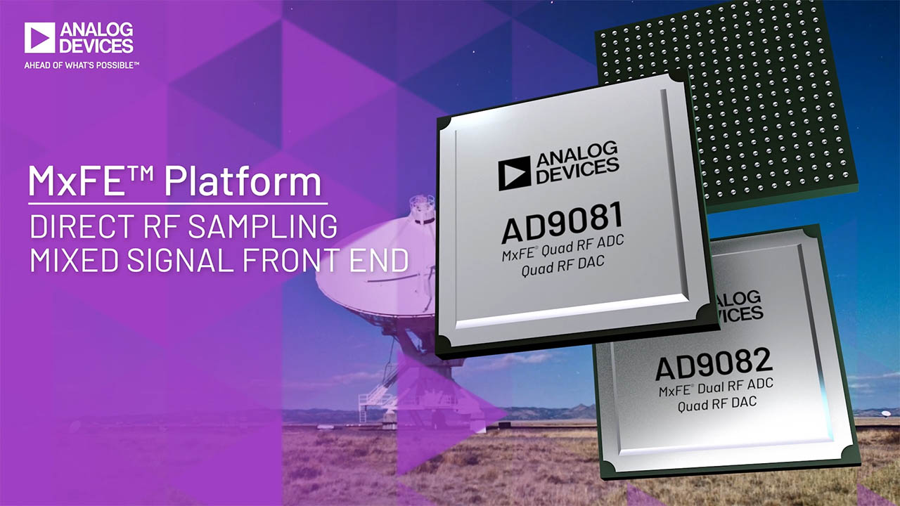
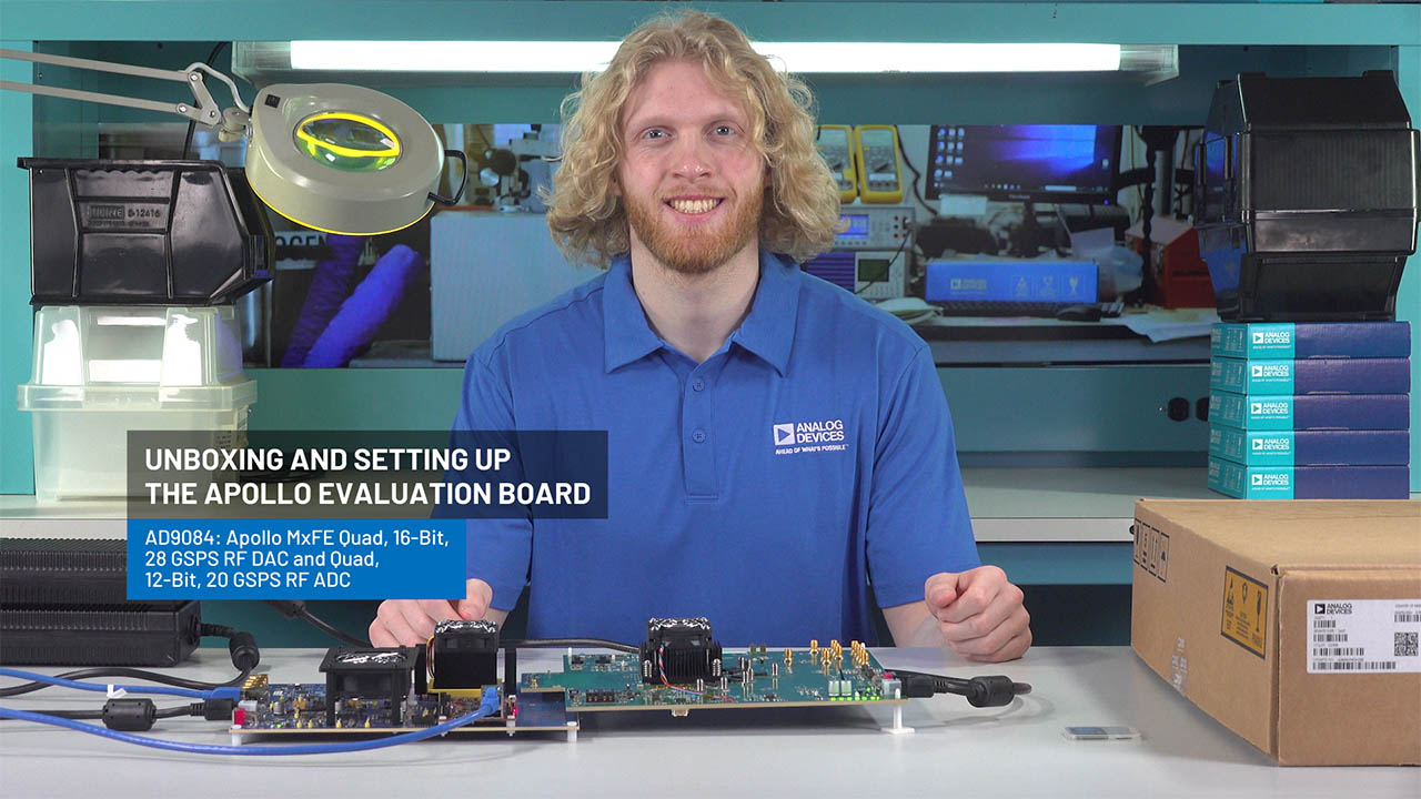
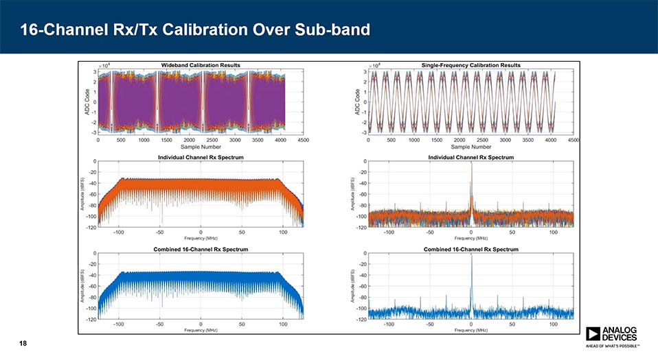
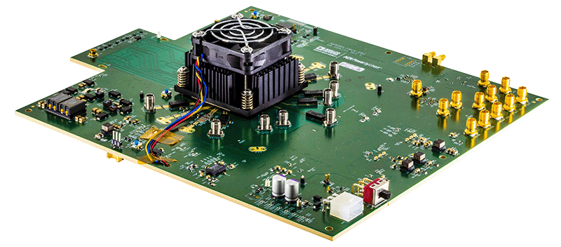
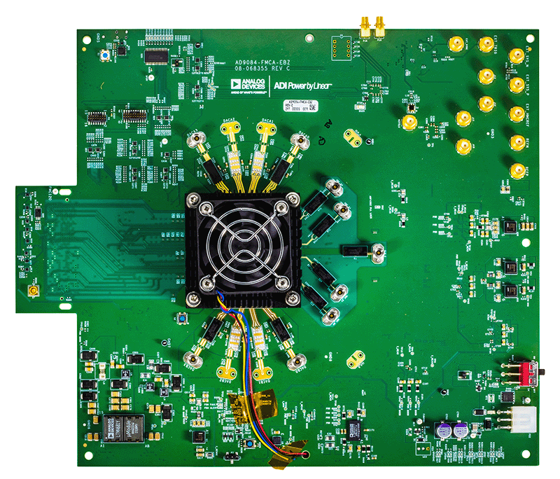
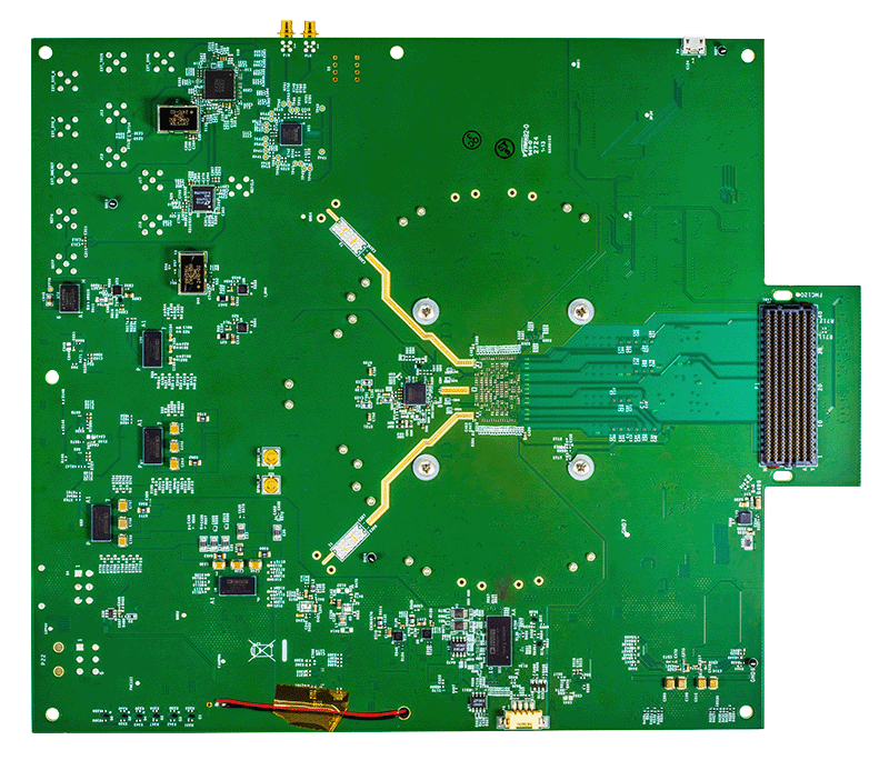
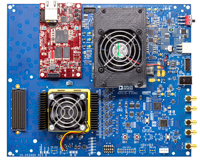
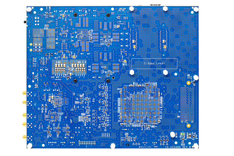
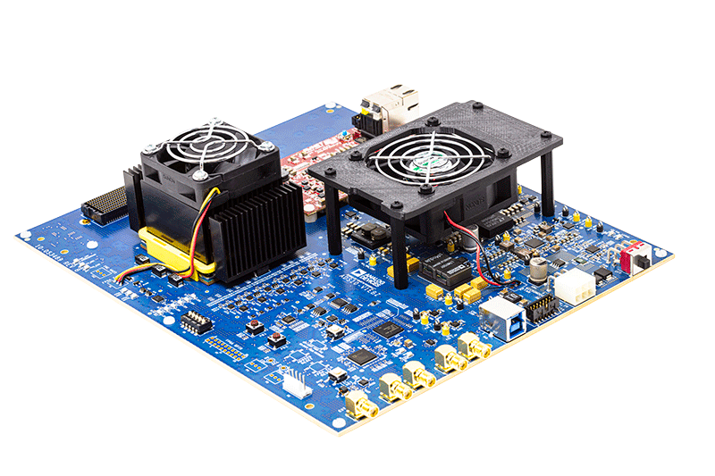
The Apollo mixed signal front-end (MxFE®) is a highly integrated device with a 16-bit, 28 GSPS maximum sample rate, RF digital-to-analog converter (DAC) core, and 12-bit, 20 GSPS maximum sample rate, RF analog-to-digital converter (ADC) core. The AD9084 supports four transmit channels and four receive channels. The AD9084 is well suited for applications requiring both wideband ADCs and DACs to process signal(s) having wide instantaneous bandwidth. The device features a 48 lane, 32.5 Gbps JESD204C or 20 Gbps JESD204B data transceiver port, an on-chip clock multiplier, and a digital signal processing (DSP) capability targeted at either wideband or multiband, direct to RF applications. The AD9084 also features a bypass mode that allows the full bandwidth capability of the ADC and/or DAC cores to bypass the DSP datapaths. The device also features low latency loopback and frequency hopping modes targeted at phased array radar systems and electronic warfare applications.
The AD9084 is available in a 24 mm x 26 mm, 899-ball BGA and operates within the –40°C to +110°C junction temperature range. For additional information, contact ApolloSupport@analog.com.
APPLICATIONS
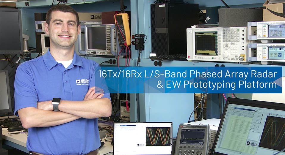
- Radar and communications
- L/S/C/X/Ku band radar and electronic warfare
- Phase array system
- Broadband communications systems
- Electronic test and measurement systems
- Satellite communications
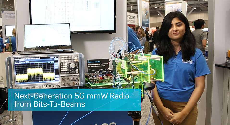
- Microwave point-to-point, X-band and 5G mmWave
Thank you for showing interest in Apollo MxFE™ and our upcoming AD9084/AD9088 product release! Subscribe to stay on top of Apollo news, TODAY!
参考资料
数据手册 2
用户手册 2
应用笔记 1
设计笔记 1
技术文章 19
视频 19


产品选型指南 1
第三方解决方案 1
FPGA 互操作性报告 5
器件驱动器 4
模拟对话 3
这是最新版本的数据手册
软件资源
API Device Drivers 1
Device Application Programming Interface (API) C code drivers provided as reference code that allows the user to quickly configure the product using high-level function calls. The library acts as an abstraction layer between the application and the hardware. The API is developed in C99 to ensure agnostic processor and operating system integration. Customers can port this application layer code to their embedded systems by integrating their platform-specific code base to the API HAL layer.
To request this software package, go to the Software Request Form signed in with your MyAnalog account and under “Target Hardware” select “High Speed Data Converters” and choose the desired API product package. In addition, there are two SW packages available specifically for Apollo MxFE™. There is a PyApp/ACE evaluation package and there are FPGA bin files supporting various use cases. You will receive an email notification once the software is provided to you.
器件驱动器 5
Evaluation Software 1
JESD204x Frame Mapping Table Generator
The JESD204x Frame Mapping Table Generator tool consists of two Windows executables that will allow the user to input any valid combination of JESD204x parameters (L, M, F, S, NP) in order to output a .csv file that illustrates the frame mapping of the JESD204x mode in table format. There is an executable that allows the user to input a single JESD204x mode and another, that allows the user to input the parameters for multiple JESD204x modes in a specified .csv format in order to output a .csv file that illustrates the frame mapping of each of the JESD204x modes that were input into separate tables.
硬件生态系统
| 部分模型 | 产品周期 | 描述 |
|---|---|---|
| ADF4030 | 预发布 | 10 通道精密同步器 |
| LDO Linear Regulators 2 | ||
| LTM4709 | 推荐新设计使用 | 具有可配置输出阵列的三通道 3A、超低噪声、高 PSRR、超快速 μModule 线性稳压器 |
| LT3094 | 推荐新设计使用 | −20V、500mA、超低噪声、超高 PSRR 负线性稳压器 |
| Phase-Locked Loop (PLL) Synthesizers 2 | ||
| ADF4382 | 预发布 | 集成 VCO 的微波宽带频率合成器 |
| ADF4382A | 推荐新设计使用 | 适用于高性能转换器时钟应用的 2.87GHz 至 21GHz 小数 N PLL/VCO |
| Power System Management (PSM) & Sequencers 1 | ||
| LTC2977 | 推荐新设计使用 | 具准确输出电压测量功能的 8 通道 PMBus 电源系统管理器 |
| RF VGAs (Variable Gain Amplifiers) 2 | ||
| ADL6331 | 预发布 | 0.38 GHz 至 12 GHz TxVGA |
| ADL6332 | 预发布 | 0.38 GHz 至 12 GHz RxVGA |
| 开关稳压器 3 | ||
| LT8627SP | 推荐新设计使用 | 具有超低噪声的18V/16A降压型Silent Switcher 3 |
| LTM4702 | 推荐新设计使用 | 16VIN 8A 超低噪声 Silent Switcher μModule 稳压器 |
| LTM8074 | 推荐新设计使用 | 40VIN 1.2A Silent Switcher µModule 稳压器 |
工具及仿真模型
Coherent Sampling Calculator
Calculate coherent sampling frequency and coherent input frequency
打开工具折频工具
该工具展示了输入信号及其谐波通过ADC实现数字化时的混叠效应。用户可选择单音或调制载波输入信号,并观察多达10个奈奎斯特区域内的混叠效应。
打开工具ADIsimPLL™
ADIsimPLL可以对ADI公司最新的高性能PLL产品进行快速、可靠的评估。它是目前最全面的PLL频率合成器设计和仿真工具,可实现所有对PLL性能有显著影响的重要非线性效应仿真。ADIsimPLL可以免去设计过程中的至少一项重复劳动,从而加快上市速度。
打开工具SNR/THD/SINAD计算器
此计算器可将SNR、THD和SINAD转换为ENOB和噪声。 它还能根据SNR、THD或SINAD中的两个参数计算另一个参数。
打开工具Clock & Timing Tools
Analog Devices provides design tools that work with our product portfolio to help engineers build critical clock and timing IC solutions for wired and wireless networks.
打开工具Data Conversion Calculator
Calculate ENOB, SNR, SINAD, THD.
打开工具热模型 2
S-参数 2
IBIS 模型 1
AD9081/AD9082/AD9986/AD9988 AMI Model
打开工具High Speed Converter Toolbox for MATLAB
打开工具评估套件
最新评论
需要发起讨论吗? 没有关于 AD9084的相关讨论?是否需要发起讨论?
在EngineerZone®上发起讨论