Power

- Battery Management
- Charge Pumps
- Circuit Monitors
- Fan Speed & TEC Controllers
- Hot Swap Controllers
- Lamp & Tube Drivers
- LED Drivers
- Linear Regulators
- �Module Regulators
- MOSFET & Gate Drivers
- POE Controllers
- Power System Managers & Sequencers
- Protection Switches & Controllers
- Supervisors & Resets
- Switching Regulators & Controllers
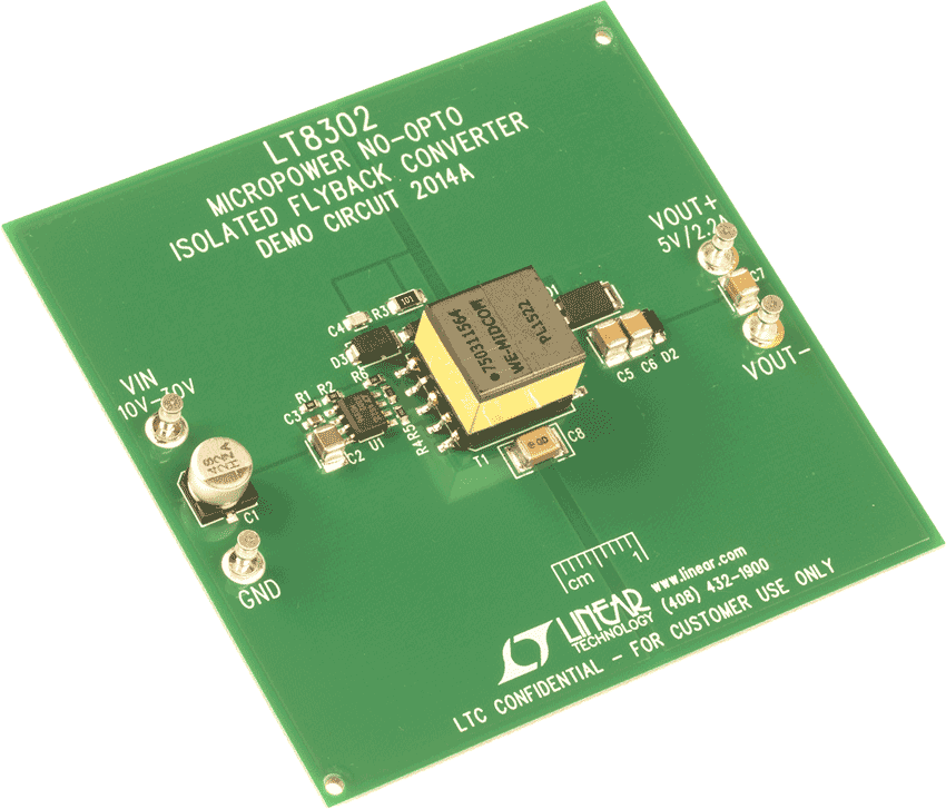
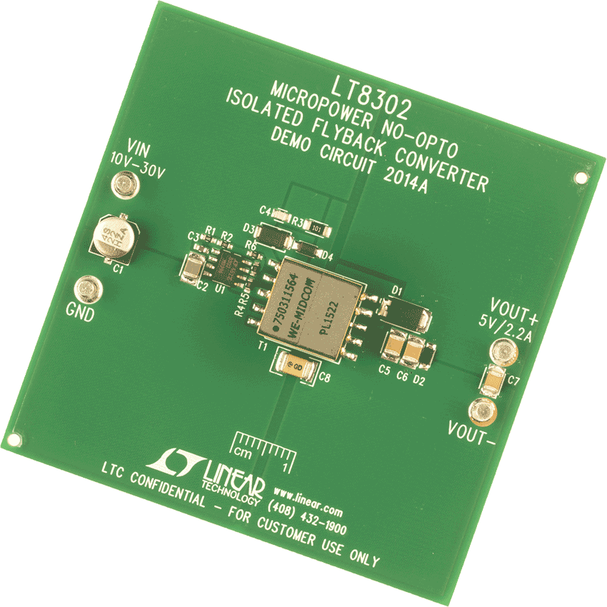
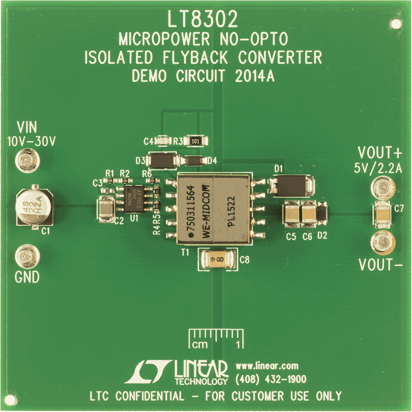
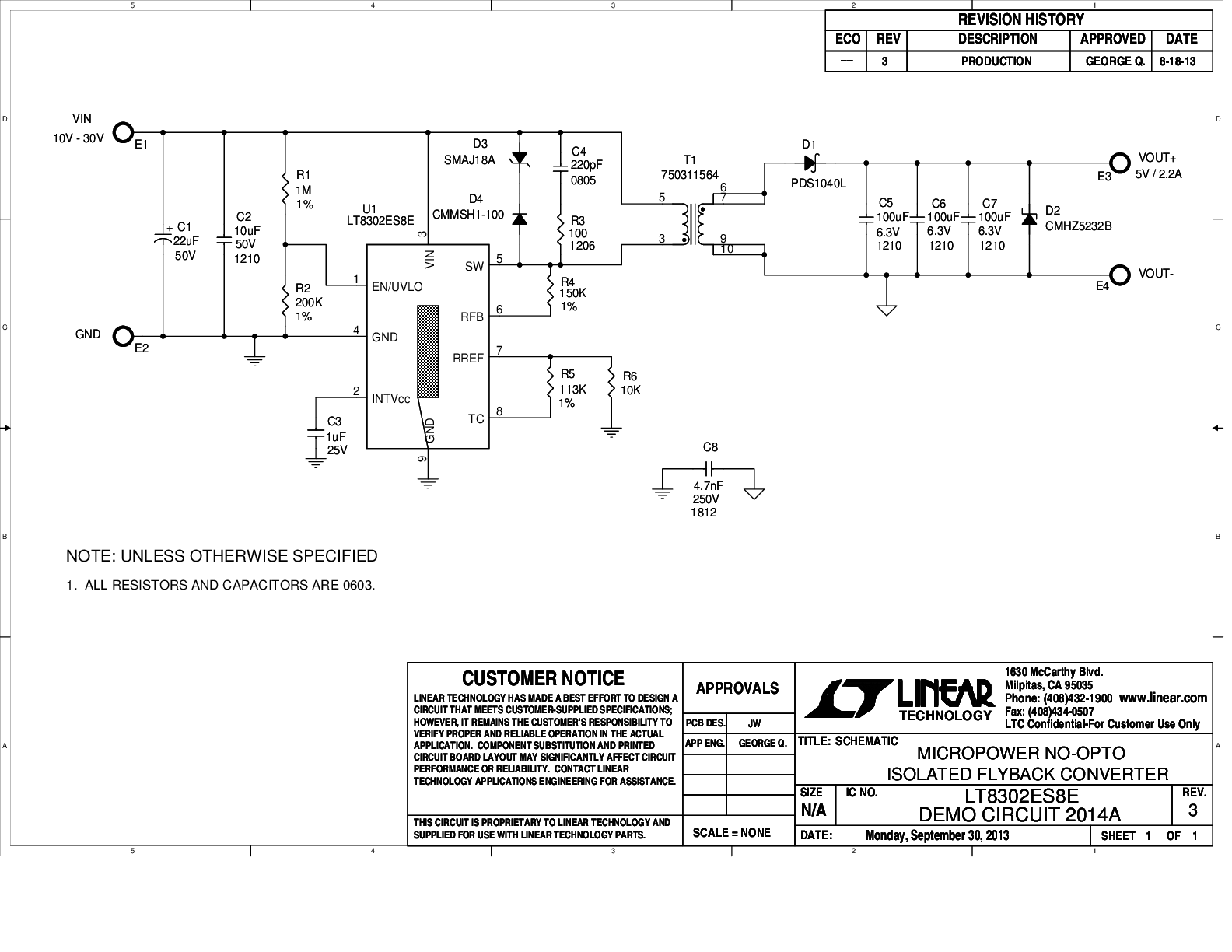
LT8302/LT8302-3